Conductive Nanoparticle Inks for Printed Electronics and Biosensors
Abstract
The rapid advancement of digitally printed electronics has increased demand for conductive nanomaterials that combine fine-feature patterning, strong electrical performance, and scalable manufacturing. Gold and silver nanoparticle inks (NPIs) address these requirements across inkjet and aerosol jet printing platforms.
The following sections outline the materials framework, processing compatibility, electrical performance, and application relevance of six commercially available formulations: gold (25 wt% Au, 40 wt% Au, 62-72 wt% Au) and silver (25 wt% Ag, 40 wt% Ag, 65 wt% Ag) NPIs. Particular focus is given to biosensing, radio frequency (RF) structures, miniaturized electronics, and research-to-production scalability.
Introduction
Additive manufacturing enables the fabrication of electronic devices for applications spanning defense, biomedical technologies, and RF systems. Digital printing methods, such as drop-on-demand inkjet and aerosol jet printing, support mask-free deposition of conductive materials across a range of substrates. Material properties strongly influence device performance, with conductivity after curing, adhesion, and long-term stability representing key considerations. Ink formulation and processing parameters further affect feature definition, print consistency, and device functionality. The gold and silver NPIs presented here are compatible with both inkjet and aerosol jet printing and produce uniform conductive patterns. Figure 1 illustrates representative conductive patterns printed with gold nanoparticle inks and highlights fine-feature resolution and pattern uniformity. The inks are compatible with multiple substrate types, including polymeric materials used in wearable electronics, and support relatively low-temperature processing for diverse manufacturing requirements.
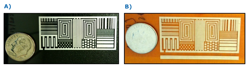
Figure 1. (A) Inkjet-printed 25 wt% Ag silver conductive patterns on glass, showing fine-line and grid structures, with a coin for scale. (B) Inkjet-printed 40 wt% Au gold conductive patterns on glass, demonstrating fine-feature resolution and pattern uniformity, shown alongside a coin for scale.
Key advantages
These products are designed to solve common challenges in research and development (R&D) and early-stage production environments by delivering a combination of performance, flexibility, and scalability. These high-performance conductive inks consistently perform across platforms and scale predictably from lab to production.
Table 1. Key advantages of NPIs for digital electronics manufacturing.
Materials overview
Portfolio summary
The silver and gold NPIs target specific digital printing methods and application classes (as referenced in Table 2). The silver series includes 25 wt% Ag, formulated for fine conductive traces and compatible with both inkjet and aerosol jet printing platforms; 40 wt% Ag provides higher metal loading to achieve increased conductivity; and 65 wt% Ag, optimized specifically for pneumatic aerosol jet printing systems and is well-suited for 3D and conformal patterning on complex surfaces.
The gold series includes 25 wt% Au, developed for biosensors and microelectrode fabrication and compatible with both inkjet and aerosol jet systems; 40 wt% Au, optimized for structures requiring enhanced conductivity; and 62–72 wt% Au targets high-density electrode arrays where precision and electrical performance are critical.
Table 2. Conductive NPIs, their target applications, viscosity and surface tension.
Printing compatibility
Inkjet printing
25 wt % Au and 25 wt% Ag nano-ink products were engineered for drop-on-demand inkjet systems, where stable droplet formation depends on maintaining viscosity and surface tension within appropriate operating windows. Rheological characterization confirms that all six formulations fall within appropriate operating windows for their respective printing platforms. Table 2 summarizes measured viscosity and surface tension values for each ink.
The 65 wt% Ag formulation exhibits a slightly broader range (12-20 cP) compared to the inkjet series, consistent with the higher metal loading and pneumatic atomization requirements of aerosol jet platforms. All inkjet formulations are all within the 8-14 cP window generally associated with stable drop-on-demand jetting behavior. Surface tension values for all six formulations range from 28.4 to 30.7 mN/m, within the typical operating envelope for modern piezoelectric inkjet printheads.
These inks are commonly used with nozzle diameters in the 100–300 µm range and drop spacing around 100 µm, depending on the printer platform and desired feature size.
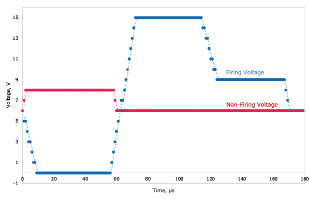
Figure 2.Typical inkjet printing waveforms for conductive gold (943878) and silver (943886) nanoinks printed with Dimatix DMP2831 inkjet printer.
Under optimized printing conditions (as referenced in Figure 2), these rheological properties support stable jetting behavior, reduced satellite droplet formation, consistent droplet morphology, and fine feature resolution. Matching ink properties with printer settings helps achieve reliable and repeatable print performance.
Aerosol jet printing
65 wt% and 25 wt% Ag and 25 wt% Au are compatible with aerosol jet deposition, enabling precise material placement for applications that require fine features and three-dimensional patterning. When processed under optimized conditions, these inks can achieve fine line widths below approximately 200 µm (depending on nozzle size and process parameters), while also supporting relatively high aspect ratio traces. Aerosol jet technology further allows conformal coating on non-planar and complex substrates, making it well suited for printing onto stepped surfaces, curved components, and integrated device architectures. Controlled overspray behavior, achieved through appropriate gas flow and nozzle configuration, helps maintain feature definition and edge clarity.
Together, these characteristics make the formulations particularly suitable for advanced packaging, 3D interconnects, embedded systems, and other applications where compact geometries, vertical integration, and precise conductive patterning are required.
Electrical performance
Following thermal sintering, nanoparticle densification results in conductive pathways approaching bulk metal performance. Figure 3 shows resistivity as a function of film thickness for the silver nanoink formulations.
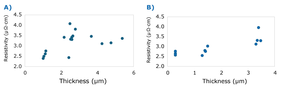
Figure 3.Resistivity versus film thickness for printed silver nanoinks on glass: (A) Conductive Silver Nanoink for Inkjet Printing (943894) and (B) Conductive Silver Nanoink for Inkjet Printing (943886).
Silver inks
Following thermal sintering, nanoparticle densification promotes the formation of continuous conductive pathways. Inkjet printed silver-based films on glass substrates demonstrate resistivity values consistently within the 2.5-4.4 µΩ·cm range across 25 wt% Ag and 65 wt% Ag formulations when cured at 250 °C for one hour. For reference, bulk silver has a resistivity of approximately 1.59 µΩ·cm.
A key finding from characterization is that resistivity performance is independent of silver solid loading. All three formulations converge to equivalent resistivity at approximately 2 µm film thickness, indicating that film formation quality is the primary determinant of electrical performance rather than metal content.
Aerosol jet-deposited silver films show modestly higher resistivity than inkjet-printed films of equivalent thickness, consistent with the different film formation mechanisms of the two deposition methods. Notably, AJP silver film resistivity shows minimal dependence on film thickness, unlike the inkjet-printed series.
For applications with substrate thermal budget constraints, low-temperature sintering profiles remain viable but require extended cure times. Silver Inks need a minimum of 200 °C with a curing time of 30 minutes, and gold inks need a minimum temperature of 250 °C for 30 minutes. Extended cure times beyond 90 minutes at 140 °C did not show further improvement and are not recommended, likely due to incomplete sintering under short thermal budgets. The resistance of either Ink does not significantly change with increased time or temperature.
Gold inks
These gold inks are designed to achieve reliable electrical performance following thermal sintering, with bulk gold having a resistivity of approximately 2.44 µΩ-cm. Inkjet printed gold films on glass substrates exhibit a stronger thickness-dependent resistivity relationship than the silver series. 40 wt% Au cured at 300 °C for one hour demonstrates resistivity values of approximately 5-14 µΩ-cm across measured thickness, with a strong linear correlation (R² = 0.95) between film thickness and resistivity. 25 wt% Au cured at 250°C for 1 hour shows a similar trend with a broader range of approximately 4–21 µΩ-cm (R² = 0.91).
These results indicate that for gold inks, controlling film thickness is critical to achieving target electrical performance. Thinner, more uniform films are recommended for applications requiring minimum resistivity. Aerosol jet deposition of gold inks produces lower resistivity at equivalent or greater film thickness compared to ink jet, suggesting improved film densification via the AJP process. Users should optimize sintering conditions and film thickness based on their specific substrate, application, and target resistivity requirements.
Substrate compatibility
These conductive inks are compatible with a broad range of electronic substrates supporting both rigid and flexible device architectures. These include polyimide (PI), which is widely used in flexible circuits due to its thermal stability, as well as traditional rigid substrates such as glass and silicon for sensors, microelectronic, and RF applications. The inks are also suitable for flexible laminates used in multilayer flexible hybrid electronics and conformal systems.
Several processing factors influence adhesion performance, most notably the surface energy of the substrate and the curing profile used after deposition. Surface treatments such as plasma or corona processing can improve wetting and interfacial bonding, while optimized thermal curing conditions help promote proper nanoparticle sintering and film densification. Together, substrate preparation and controlled curing promote strong adhesion, high conductivity, and long-term reliability.
For the silver ink series, both 25 wt% Ag and 40 wt% Ag achieve a 5B adhesion rating on PI substrates across tested film thickness. 65 wt% Ag similarly achieves a 5B rating rating on PI; on silicon substrates, 5B adhesion is achieved conditionally for films below approximately 3 µm in thickness, beyond which adhesion may degrade. Users depositing thicker 65 wt% Ag films on silicon are advised to validate adhesion performance for their specific process conditions.
For the gold ink series, adhesion on PI is also excellent but exhibits a stronger film thickness dependence. 25 wt% Au achieves 5B adhesion on PI for films below approximately 2 µm; 40 wt% Au achieves 5B adhesion on PI for films below approximately 1 µm. In both cases, exceeding these thickness thresholds may result in reduced adhesion scores, and optmising deposition parameters to maintain film thickness within these ranges is recommended for mechanically demanding applications.
Together, these results demonstrate that silver and gold ink portfolio delivers excellent, process-ready adhesion on polyimide, the most commonly used flexible substrate in printed and wearable electronics, without requiring additional adhesion promoters or surface functionalization. This out-of-the-box compatibility with PI represents a meaningful practical advantage for product development teams, reducing process complexity and enabling faster design-to-fabrication cycles. Adhesion on other types of substrates is still currently being tested and evaluated.
Application
Printed biosensors
Gold NPIs serve as conductive materials for printed biosensors, offering unique advantages for electrochemical and biofunctionalized sensor platforms. Their chemical and physical properties make them particularly well-suited for devices where precision, stability, and biocompatibility are essential.
Gold electrodes enable strong thiol-based surface chemistry, which allows biomolecules such as enzymes, antibodies, and deoxyribonucleic acid (DNA) strands to be reliably attached. They also provide a stable electrochemical response, excellent resistance to oxidation, and inherent biocompatibility, properties that are critical for accurate and durable biosensing performance.
Recent research has highlighted the growing role of inkjet-printed gold electrodes in low-resource biosensing contexts, with well-characterized thiol chemistry enabling self-assembled monolayer functionalization and compatibility with multiplexed sensor platforms.1 These characteristics make gold NPIs ideal for a wide range of applications, including enzymatic glucose sensors, immunoassay platforms, DNA and ribonucleic acid (RNA) detection arrays, wearable physiological monitors, and lab-on-chip microelectrode systems. By combining printability with these functional advantages, gold inks support the development of compact, flexible, and high-performance biosensing devices.
Digital Fabrication Advantages
Inkjet-printed gold electrodes offer several significant advantages over traditional subtractive lithography, particularly for the development of next-generation biosensors. By enabling rapid design iteration, these inks allow researchers and engineers to quickly modify and optimize electrode layouts without the need for new masks or tooling. Mask-free fabrication also reduces process complexity, while targeted deposition minimizes material waste compared to conventional etching processes.
In addition to these manufacturing benefits, these gold inks deliver strong electrochemical performance. Sensitivity, limit of detection, and stability over multiple cycles can be quantified once experimental data are available, allowing direct correlation between electrode design and sensor performance. The combination of fine feature resolution, chemical robustness, and compatibility with flexible substrates positions these gold inks as promising candidates for a wide range of biosensing applications, from enzymatic glucose sensors to lab-on-chip microelectrodes.
The combination of fine feature resolution and chemical robustness positions these gold inks as strong candidates for next generation biosensing platforms.
RF and electromagnetic interference (EMI) applications
Silver-based inks provide versatile solutions for high-performance electronics, particularly in applications requiring reliable conductivity and precise patterning. These inks are well suited for printed antennas, RF interconnects, and EMI shielding patterns, where accurate electrical performance and low resistance are critical. The ability to create compact conductive geometries allows designers to optimize space and integrate complex circuitry into constrained layouts. Furthermore, the fine-line resolution achievable with these inks supports the miniaturized circuit architectures that are increasingly demanded in defense electronics, advanced communication systems, and other high-density electronic platforms. By combining precision printing with high conductivity, silver inks enable both innovative designs and practical manufacturing efficiency.
The portfolio has been developed with scalability and manufacturing reliability in mind, supporting the transition from laboratory research to pilot-scale production and full commercialization. Key improvements include increased production capacity, ensuring that enough ink is available for both research and industrial use. Batch-to-batch consistency has been enhanced through standardized synthesis and quality control processes, providing predictable performance across multiple production runs. In addition, rigorous quality control measures and a reliable supply chain ensure that materials meet high technical standards and are consistently available when needed. Together, these factors make these inks a dependable choice for institutions and companies looking to move from experimental applications to scalable manufacturing of advanced electronic devices.
Conclusion
These conductive inks support digitally printed electronics from laboratory research through early-stage production. High-purity nanoparticles and controlled rheological properties contribute to consistent electrical conductivity and reproducible print performance.
The portfolio supports applications including biosensing, flexible and wearable electronics, RF systems, EMI shielding, microheaters, and miniaturized circuitry. Gold-based formulations provide chemically stable surfaces well suited for enzymatic and immunoassay sensor fabrication, while silver-based formulations enable high-conductivity traces for antennas and RF interconnects. Fine-feature patterning on flexible substrates supports rapid prototyping and iterative design.
Controlled manufacturing processes and quality protocols help maintain consistent electrical and mechanical properties across production batches.