Organic Materials for Thin Film Transistors
Flexible electronic circuits, displays, and sensors based on organic active materials will enable future generations of electronics products that may eventually enter the mainstream electronics market. The motivations in using organic active materials come from their ease in tuning electronic and processing properties by chemical design and synthesis, low cost processing based on low temperature processes and reel-to-reel printing methods, mechanical flexibility, and compatibility with flexible substrates.1,2
Organic Thin Film Transistors
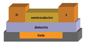
Organic thin film transistors (OTFTs) are the basic building blocks for flexible integrated circuits and displays. A schematic structure is shown in Figure 1. During the operation of the transistor, a gate electrode is used to control the current flow between the drain and source electrodes. Typically, a higher applied gate voltage leads to higher current flow between drain and source electrodes. The semiconductor material for a fast switching transistor should have high charge carrier mobility and on/off current ratio. For pixel switching transistors in liquid crystal displays, mobility greater than 0.1 cm2/Vs and on/off ratio greater than 106 are needed.

Figure 1.Schematic structure of an organic thin film transistor (OTFT). S: source; D: drain.
To make OTFTs, materials ranging from conductors (for electrodes), semiconductors (for active channel materials), to insulators (for gate dielectric layers) are needed. This article will discuss the basic requirements for these materials and give examples of some representative materials.
Organic Semiconductors
There are two types of organic semiconductors based on the type of majority charge carriers: p-type (holes as major charge carriers) and n-type (electrons as major charge carriers). To facilitate charge transport, the organic semiconductor layer usually consists of π-conjugated oligomers or polymers, in which the π–π stacking direction should ideally be along the current flow direction. This requires the semiconductor molecules to self-assemble into a certain orientation upon either vapor or solution deposition. It is also important that the semiconductor thin film has large, densely packed and well-interconnected grains. Most small molecule, high performance organic semiconductors tend to have the long axes of the molecules oriented close to normal to the dielectric surface (Figure 2a) with the typical grain size in the order of at least a few micrometers. In case of solution processed semiconducting polymers, it is preferred for the π-conjugated plane to adapt an edge-on orientation on the surface (Figure 2b).
Figure 2.Molecular orientation of high-performance organic semiconductors. (a) Pentacene molecules assemble with the long axis oriented perpendicular to the dielectric surface. (b) Molecules of regioregular poly(3-hexylthiophene) (P3HT) spontaneously assemble into ordered structures with edge-on orientation. The π–π stacking between polymer chains facilitates charge transport.
The morphology of the semiconductor film is highly dependent on the chemical and physical nature of the dielectric surface. Patterning of dielectric surface can lead to selective patterning of the organic semiconductor in desired locations, which is important to reduce cross talk between devices. With proper control of the dielectric surface, arrays of organic semiconductor single crystals can be patterned over a large area for high performance transistors.3
Great progress has been made in the development of organic semiconductor materials. The initial demonstration of transistor activity in these films was with a narrow group of p-channel thiophene oligomers and polymers. The reported mobilities were on the order of 0.01–0.1 cm2/Vs.4,5 During the last few years, a much broader selection of molecular solids and polymers has been developed, all with mobilities above 0.1 cm2/Vs and achievable on/off ratios greater than 105.1 The chemical structures of some representative materials are shown in Figure 3. p-Channel compounds in this category include substituted thiophene oligomers, pentacene, acenes, and their derivatives, phthalocyanine- and thiophene-based fused ring compounds, and fluorene oligomer derivatives. Regioregular poly(3-hexylthiophene) is one of the few polymer semiconductors that spontaneously assembles into well ordered structures upon solution deposition by drop casting or spin coating6 (Figure 3) and gives a mobility greater than 0.1 cm2/Vs.7,8 More recently, a few new polythiophene derivatives have been reported and show improved mobility and air stability (Figure 3, g,h).9,10
Figure 3.Chemical structures of some representative p-channel organic semiconductors. (a) pentacene; (b) tetraceno[2,3-b]thiophene; c) TIPS-pentacene; (d) asexithiophene; (e) oligothiophene-fluorene derivative; (f) regioregular(poly3-hexylthiophene); (g) poly(3,3’’’-didodecylquaterthiophene); (h) poly(2,5-bis(3-decylthiophen-2-yl)thieno[3,2- b]thiophene).
Complementary metal oxide semiconductor (CMOS) circuits are desirable because of their ease in circuit design and low power consumption. CMOS inverters usually consist of a p- and an n-channel transistor. Several classes of organic materials have displayed good n-channel activity, including C60, perfluoro-copper phthalocyanine, and naphthalene and perylene-based compounds.17,18,19,20 Figure 4 shows the chemical structures of some representative high performance air-stable n-channel semiconductors. More recently, ambipolar behavior for certain organic semiconductors has also been reported.21 This type of material can be used for the fabrication of complementary circuits without the need to pattern the p- and n-channel semiconductors separately.
Figure 4.Chemical structures of some representative n-channel organic semiconductors. (a) C60; (b) hexadecafluoro copper phthalocyanine (F16CuPc); (c) naphthalene diimide derivative; (d) perylene diimide derivative.
Dielectric Materials
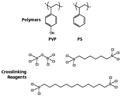
The dielectric layer for organic transistors should be as thin as possible, pinhole-free, and ideally with a high dielectric constant for low voltage operation. Inorganic, organic, and inorganic/organic hybrid materials have been investigated as the gate dielectric materials. Promising materials include poly(methy methacrylate) (PMMA), poly(styrene), poly(vinyl phenol), silsesquioxane (glass resin), and benzocyclobutene (BCB), etc. (Figure 5a).23,24,25 Crosslinked polymers generally are more robust as ultrathin dielectric materials.26 Examples of cross-linkers used to make dielectric materials are shown in Figure 5b. Even a well-ordered densely packed self-assembled monolayer (SAM) may be used as the thinnest possible high quality dielectric layer.27 Incorporation of high dielectric constant inorganic nanoparticles into a polymer matrix boosts the overall dielectric constant of the thin film.28

Figure 5.Examples of dielectric materials and cross-linkers. Siloxane crosslinkers can be used to enhance stability of PVP (polyvinylphenol) and PS (polystyrene) gate insulating layers.
Surface treatment of the dielectric layer is an important method to improve organic transistor performance. Most of the charge carriers induced in the semiconductor layer are confined to the first 5 nm of the organic semiconductor film adjacent to the semiconductor/dielectric interface. Thus, the chemical and physical characteristics of the dielectric surface have a significant effect on the charge carrier transport. For example, Si-OH groups on SiO2 surface (a typical dielectric material) are known to trap electrons. Capping SiO2 surfaces with octadecyl trichlorosilane (OTS, Prod. No. 104817) molecules can significantly reduce electron traps and improve mobility of n-channel semiconductors (electrons are the major charge carriers).23
Additionally, dielectric surface treatment with SAMs also affects the nucleation and growth of organic semiconductors.29 For example, pentacene is an organic semiconductor with the highest reported thin film charge carrier mobility. Its charge carrier mobility changes significantly depending on the types of hydrophobic SAM surface treatment of the dielectric. This difference is related to the morphological difference of the first pentacene monolayer formed on different surfaces.29
Electrode Materials
For organic transistors to function properly, charge injection from the electrode needs to be efficient. This requires the work function of the electrode to match well with the energy level of the organic semiconductor such that the energy barrier for charge injection is low. Typically high work function electrodes (Au, Pd, or indium tin oxide) have been used for p-channel organic transistors. Electrode surface modification with a self-assembled monolayer can be used to improve the charge injection into the organic semiconductor.30 When the organic semiconductor is deposited onto the source and drain electrodes, the morphology of organic semiconductors is significantly different when deposited on SAM-modified Au compared to bare Au. This observation has been used to tune the morphology of the organic semiconductor at the Au/ organic interface to improve its charge injection.31
Solution processable electrode materials are desirable for low cost production. To that end, a few groups have developed Au or Ag nanoparticle inks that can be cured at below 200 °C to be compatible with low cost plastic substrates.32 Carbon nanotube dispersion and conducting polymer solutions are among other promising electrode candidates.
In summary, organic materials are promising candidates for flexible electronic devices. Significant progress has already been made in this field. Nevertheless, better understanding of the structure property relationship is still needed so that we can rationally design materials to achieve desired device performance parameters.
Related Products
References
To continue reading please sign in or create an account.
Don't Have An Account?