357294
铟
foil, thickness 0.25 mm, 99.99% trace metals basis
别名:
Indium element
登录并加购,请在购物车里查看协议价、货期和发货地。
选择规格
变更视图
关于此项目
经验公式(希尔记法):
In
化学文摘社编号:
分子量:
114.82
NACRES:
NA.23
PubChem Substance ID:
UNSPSC Code:
12141719
EC Number:
231-180-0
MDL number:
vapor pressure
<0.01 mmHg ( 25 °C)
Quality Segment
assay
99.99% trace metals basis
form
foil
composition
In
reaction suitability
core: indium
resistivity
8.37 μΩ-cm
thickness
0.25 mm
mp
156.6 °C (lit.)
density
7.3 g/mL at 25 °C (lit.)
SMILES string
[In]
InChI
1S/In
InChI key
APFVFJFRJDLVQX-UHFFFAOYSA-N
General description
Indium foil is widely used in nuclear facilities to capture thermal neutrons, because it shows a high cross section of neutron capture reaction. Hence, it may be used in dosemeters to measure exposure. Indium foils were studied for simultaneous monitoring neutron and photon intensities in a reactor core.
Application
- High sodium ionic conductivity in PEO/PVP solid polymer electrolytes with InAs nanowire fillers.: Explores the enhancement of ionic conductivity in polymer electrolytes through the incorporation of indium arsenide nanowires, offering significant implications for battery efficiency ( Devi et al., 2021).
- A Corrosion-Resistant and Dendrite-Free Zinc Metal Anode in Aqueous Systems.: Introduces a corrosion-resistant indium-containing anode design for aqueous batteries, which prevents dendrite formation and enhances overall battery safety ( Han et al., 2020).
Preparation Note
4.6g = 50×50mm;18.4g = 100×100mm;41.4g = 150×150mm
Still not finding the right product?
Explore all of our products under 铟
signalword
Danger
hcodes
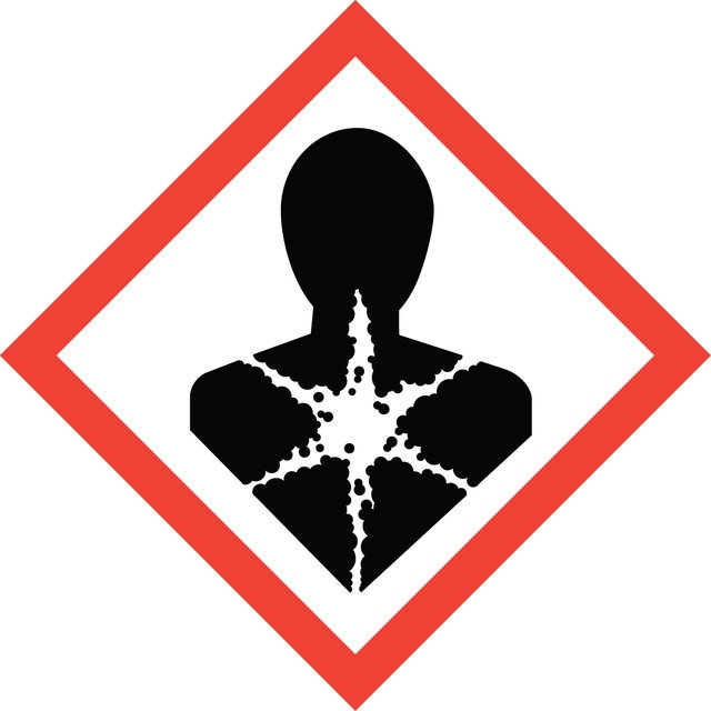
Hazard Classifications
STOT RE 1 Inhalation
target_organs
Lungs
存储类别
6.1C - Combustible acute toxic Cat.3 / toxic compounds or compounds which causing chronic effects
wgk
WGK 1
flash_point_f
Not applicable
flash_point_c
Not applicable
ppe
dust mask type N95 (US), Eyeshields, Gloves