产品名称
单层石墨烯薄膜, 1 cm x 1 cm on SiO2/Si substrate, avg. no. of layers, 1
Quality Segment
form
film
feature
avg. no. of layers 1
resistance
600 Ω/sq
L × W × thickness
1 cm × 1 cm × (theoretical) 0.345 nm, monolayer graphene film, 1 cm × 1 cm × 525 μm, SiO2/Si substrate
General description
石墨烯是一种独特的单原子厚度的石墨,以二维结构存在的碳的同素异形体。在所有合成技术中,石墨烯在各种基质上的化学气相沉积是大规模生产高质量石墨烯的最有前景的方法。 沉积在介电表面上的石墨烯在石墨烯FET中可能会表现出更好的性能。可以利用牺牲层铜薄膜通过直接化学气相沉积,使石墨烯沉积在SiO2/Si上。
方块电阻测量在真空室中进行,在四点结构(范德堡法,银漆接触)内注入超过 10uA的电流以确保其可重复性
石墨烯膜
生长方式:CVD合成
转移方式:干净的转移方式
质量控制:光学显微镜检查 & 拉曼检查
尺寸:1 cm x 1 cm
外观(颜色):透明
透明度:>97%
外观(形式):薄膜
覆盖率: >95%
石墨烯层数:1
厚度(理论上):0.345 nm
Al2O3上的FET电子迁移率:2; 000 cm2/V·s
SiO2/Si上的FET电子迁移率(预期):4; 000 cm2/V·s
薄层电阻:600 Ohms/sq。
粒度:最大10 μm
底物
尺寸:1.25 cm x 1.25 cm
类型/掺杂剂:P/B
方向:100
生长方式:CZ
电阻率:1-30 ohmcm
厚度:525 +/- 25μm
前表面:抛光
背面:蚀刻
涂层:两面晶片均为300 nm热氧化层
Application
Still not finding the right product?
Explore all of our products under 单层石墨烯薄膜
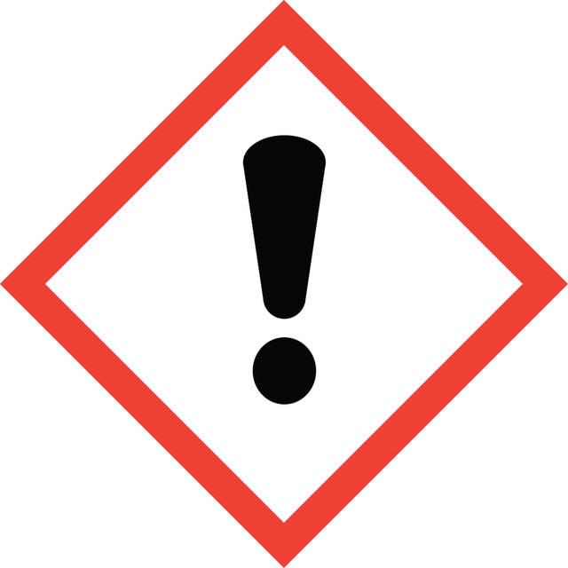
signalword
Danger
hcodes
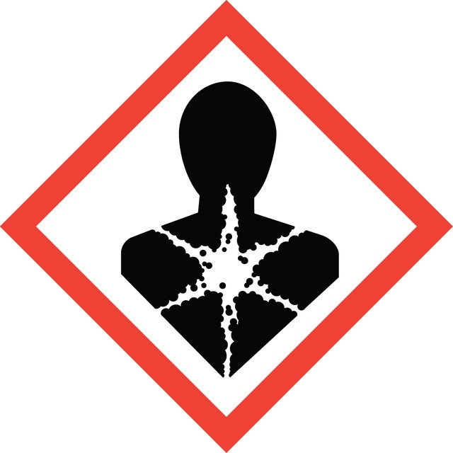
Hazard Classifications
Eye Irrit. 2 - STOT RE 1 Inhalation - STOT SE 3
target_organs
Lungs, Respiratory system
存储类别
6.1D - Non-combustible acute toxic Cat.3 / toxic hazardous materials or hazardous materials causing chronic effects
wgk
WGK 3
flash_point_f
Not applicable
flash_point_c
Not applicable