Soluble Pentacene Precursors
Fabrication of Organic Field Effect Transistor Device Using a Soluble Pentacene Precursor
In order to introduce un-functionalized pentacene within a device such as an organic field effect transistor (OFET), soluble pentacene precursors, which readily transform into pentacene upon heating (at approx 200 °C), are critically important materials. The fabrication procedure of solution-deposited bottom-gate, bottom-contact native pentacene transistors is described below and the representative performance characteristics of the transistors are presented.
Fabrication Procedure
Highly-doped n-type Si wafers (resistance <0.01 Ω-cm) with thermally grown SiO2 of thickness 250 nm are used as the substrates, which form the back-gate and gate-dielectric of the transistors, respectively. These 2 x 2 cm2 wafers are treated with oxygen plasma at 50 W (Technics PlanarEtchII-350 Plasma Generator) for 10 min. The substrates are then immediately surface-treated with HMDS (1,1,1,3,3,3-Hexamethyldisilazane, Product No. 40215). HMDS modifies the SiO2 surface and contact angle to improve transistor characteristics. A Petri dish containing HMDS (5 mL) is placed in a vacuum desiccator along with the substrates to be surface-treated. The desiccator is pumped down with a house vacuum and the substrates are exposed to HMDS vapor for 20 minutes. Source and drain electrodes of Au are then deposited on the substrates through shadow masks by e-beam evaporation.
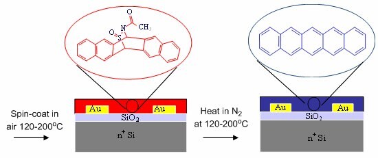
The 13,6-N-sulfinylacetamidopentacene precursors (Product No. 666025) is dissolved in chloroform (15 mg/mL) and filtered through a 0.2 µm PTFE syringe filter. A few tenths of a milliliter of the solution are then placed on each of the substrates. The substrates are spun at 1500 rpm (with an initial ramp rate of 500 rpm per sec) for 1 min. The precursor thin film is then thermally-treated on a preheated hot plate at 200 °C for 1 min in a nitrogen atmosphere glove-box to convert the pentacene precursor into pentacene. The resulting pentacene thin films have a thickness of 100 nm. The details of the fabrication are shown in Figure 1.

Figure 1. Schematic of the solution deposition process involving spin-coating followed by thermal conversion of the pentacene/N-sulfinylacetamide adduct (red) to form pentacene (blue) thin film transistors.
Electrical Characterization
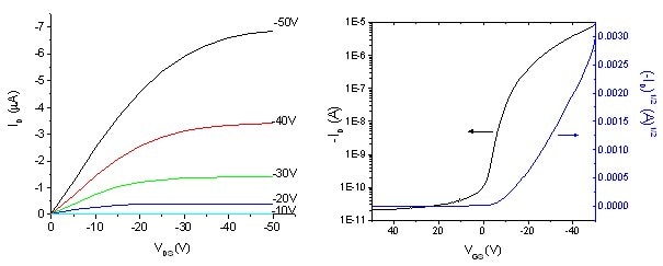
Electrical characterization of the devices is performed at ambient atmosphere using an Agilent 4156C semiconductor parameter analyzer and a Karl Suss PM5 probe station. The representative IV characteristics of the transistors fabricated are shown in Figure 2.

Figure 2. (A) Drain current (ID) versus source-drain voltage (VDS) and (B) drain current (ID) versus source-gate voltage (VGS) at a constant drain-source voltage of -50 V for a pentacene transistor fabricated from gold (15-20 nm) metal contacts and channel dimensions of L=160 µm and W=1.5 mm. The mobility is 0.189 cm2/Vs, current modulation ratio (Ion/Ioff) is 4.4 x 10⁵ and threshold voltage (VT) is -26.8 V.
The mobility (µ) and threshold voltage (VT) are calculated in the saturation regime using the square-law equation:

Where ID is the drain current, VGS is the gate-source voltage, W is the width of the channel, L is the length of the channel, µ is the mobility and VT is the threshold voltage. Mobilities of ~ 0.1-0.2 cm2 V-1 s-1 are achieved by this procedure. The SiO2/pentacene interface plays a very important role in the device characteristics and the mobilities reported can be further improved to ~1 cm2 V-1 s-1 as previously reported1,2 by vapor-prime HMDS surface treatment. Vapor-prime HMDS may be carried out in, for example, a Yield Engineering Systems tool.
In addition to the soluble pentacene precursor used above, other precusors are commercially available, such as Pentacene-N-sulfinyl-tert-butylcarbamate (Product No. 699306), which has the ability to be photopatterned using UV light in the presence of a photoacid generator before briefly heating at 130 °C. An alternative method for introducing high purity pentacene into organic electronic devices would be the use of TIPS Pentacene (Product No. 716006), a soluble pentacene molecule developed by 3M and Outrider Technologies. In conclusion, we have shown that high performance devices can be made from both soluble pentacene derivatives as well as soluble pentacene precursors. These methods are critical, as they allow researchers to overcome the insolubility of pentacene and incorporate high-mobility pentacene into their end devices.
Materials
References
To continue reading please sign in or create an account.
Don't Have An Account?