Skip to Content
Merck
CN

651486

Gallium arsenide

(single crystal substrate), <100>, diam. × thickness 2 in. × 0.5 mm

Synonym(s):

Gallium monoarsenide

Sign In to View Organizational & Contract Pricing.

Select a Size

Change View

About This Item

Linear Formula:
GaAs
CAS Number:
Molecular Weight:
144.64
NACRES:
NA.23
PubChem Substance ID:
UNSPSC Code:
12352300
EC Number:
215-114-8
MDL number:
Technical Service
Need help? Our team of experienced scientists is here for you.
Let Us Assist


form

(single crystal substrate)

resistivity

≥1E7 Ω-cm

diam. × thickness

2 in. × 0.5 mm

density

5.31 g/mL at 25 °C (lit.)

semiconductor properties

<100>

SMILES string

[Ga]#[As]

InChI

1S/As.Ga

InChI key

JBRZTFJDHDCESZ-UHFFFAOYSA-N

General description

Mobility >=4500 cm2 · V-1 · S-1
Undoped (Si-type semiconductor), EPD < 5 × 104 cm-2, growth technique = LEC & HB

Physical form

cubic (a = 5.6533 Å)


Still not finding the right product?

Explore all of our products under Gallium arsenide
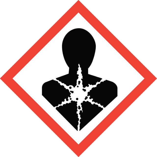

pictograms

Health hazard

signalword

Danger

Hazard Classifications

Carc. 1B - Repr. 1B - STOT RE 1

target_organs

Respiratory system,hematopoietic system

Storage Class

6.1A - Combustible acute toxic Cat. 1 and 2 / very toxic hazardous materials

wgk

WGK 3

flash_point_f

Not applicable

flash_point_c

Not applicable

Regulatory Information

危险化学品

This item has


Choose from one of the most recent versions:

Certificates of Analysis (COA)

Lot/Batch Number

Don't see the Right Version?

If you require a particular version, you can look up a specific certificate by the Lot or Batch number.

Already Own This Product?

Find documentation for the products that you have recently purchased in the Document Library.

Visit the Document Library


Protocols

Photoresist kit offers pre-weighed chemical components for lithographic processes, with separate etchants for various substrate choices.

Articles

Spintronics offer breakthroughs over conventional memory/logic devices with lower power, leakage, saturation, and complexity.


Shih-Wei Tan et al.
PloS one, 7(11), e50681-e50681 (2012-12-12)
Characterization and modeling of metal-semiconductor-metal (MSM) GaAs diodes using to evaporate SiO₂ and Pd simultaneously as a mixture electrode (called M-MSM diodes) compared with similar to evaporate Pd as the electrode (called Pd-MSM diodes) were reported. The barrier height (φ(b))
Chao-Wei Hsu et al.
Nanotechnology, 23(49), 495306-495306 (2012-11-17)
GaAs is grown by metal-organic vapor-phase epitaxy on a 55 nm round-hole patterned Si substrate with SiO(2) as a mask. The threading dislocations, which are stacked on the lowest energy facet plane, move along the SiO(2) walls, reducing the number
Kazuue Fujita et al.
Optics express, 20(18), 20647-20658 (2012-10-06)
Device-performances of 3.7 THz indirect-pumping quantum-cascade lasers are demonstrated in an InGaAs/InAlAs material system grown by metal-organic vapor-phase epitaxy. The lasers show a low threshold-current-density of ~420 A/cm2 and a peak output power of ~8 mW at 7 K, no


Global Trade Item Number

SKUGTIN
651486-1EA04061832732602