Organic Transistors for Biomedical Applications
Introduction
There is widespread demand for thin, lightweight, and flexible electronic devices such as displays, sensors, actuators, and radio-frequency identification tags (RFIDs). Flexibility is necessary for scalability, portability, and mechanical robustness. Various types of flexible thin-film transistors (TFTs)1-5 have been employed to realize flexible electronic devices on plastic substrates, such as solar cells,6 light-emitting diodes (LEDs),7 TFTs,8 memory devices,9-13 sensors,14 actuators,15 displays,16 and transponders.17 Therefore, mechanical flexibility of flexible electronics has been the focus of intensive research efforts in order to improve mechanical durability and obtain better fundamental understanding of electronic performance under bending stresses.
Recently, flexible electronics have seen widespread use in biomedical applications.18-22 The mechanical flexibility offered by organic circuits has been investigated to develop novel biomedical devices such as large-area sensitive catheters.5 To be integrated into medical devices, these organic electronic devices must be able to withstand sterilization conditions (involving exposure to temperatures exceeding 100 °C) in order to achieve asepsis and prevent infection. At such high temperatures organic devices generally degrade, either as a result of thermally induced oxidation of the organic semiconductor, changes in the crystal structure or morphology of thin films, or mechanical stresses induced by mismatches in the thermal expansion of the material stack within the devices. The use of organic electronic devices in biomedical applications will necessarily require a critical understanding and improvement of their thermal stability.
Herein, we demonstrate the fabrication of heat-resistant, flexible, and high-mobility organic TFTs and circuits that operate at voltages of 2 V and exhibit a field-effect mobility of 1.2 cm2/Vs. The effects of exposing these TFTs to various temperatures were systematically investigated and it was found that heat-induced changes in the electrical performance of the TFTs were negligible up to 120 °C. Heat-resistant TFTs were achieved using DNTT (dinaphtho-[2,3-b:2′,3′-f]-thieno-[3,2-b]-thiophene) (767638) as an organic semiconductor23 and a combination of a plasma-grown aluminum oxide (AlOx) layer and an alkylphosphonic acid self-assembled monolayer (SAM) as a gate dielectric.24 The effects of temperature on the crystal structure of the DNTT film and on the orientation of the alkylphosphonic molecules within the SAM were investigated using X-ray diffraction (XRD) and near edge X-ray absorption fine structure (NEXAFS) spectroscopy, respectively. The practical applicability of heat-resistant organic TFTs was demonstrated by subjecting them to standard medical sterilization procedures, including heating to 150 °C for 20 seconds or 121 °C for 20 minutes in air.25 Similarly, an electronic application, requiring operation of high-performance and heat-resistant circuits folded with an extremely small bending radius, was simulated using a very thin medical catheter that measures spatial distribution of pressure by wrapping a foldable transistor and sensor matrix around its surface in a helical structure.
Device Fabrication
Organic transistor circuits on a plastic substrate, which exhibit excellent electrical characteristics even at high temperatures, are shown in Figures 1A and 1B. Figure 1C shows a schematic of the heat-resistant TFTs fabricated using a thin AlOx/SAM gate dielectric on a flexible polyimide substrate. Chemical structures and physical appearance of DNTT (767638) and alkylphosphonic acid SAMs, n-octadecylphosphonic acid (C18-SAM) (715166) and n-tetradecylphosphonic acid (C14-SAM) (736414), are shown in Figures 1D and 1E, respectively. TFTs were fabricated by depositing a 25-nm thick aluminum layer as the gate electrode onto a 75-μm thick polyimide substrate by thermal evaporation through a shadow mask. Oxygen-plasma treatment with a plasma power of 100 W for 10 minutes was performed to oxidize the surface of the thermally evaporated aluminum, resulting in a thin AlOx layer on the gate electrode. The substrates were subsequently dipped into 5-mM solution of C18-SAM or C14-SAM in isopropyl alcohol for 16 hours to form a SAM with ~2-nm thickness.24 The combination of AlOx and SAM functions as the high-insulating gate dielectric layer. A 30-nm thick DNTT layer was then deposited by thermal evaporation to form the channel, followed by a 50-nm thick Au layer through a shadow mask to define the source/drain contacts. Finally, the entire surface of the device was encapsulated with organic/metal hybrid coatings.26
![Dinaphtho-[2,3-b:2,3-f]-thieno-[3,2-b]-thiophene (DNTT) transistors and circuit. A) Photograph of heat-resistant, flexible, and high-mobility organic transistor circuit on a plastic substrate. B) Photograph of an organic circuit that can operate in boiling water. C) Schematic cross section of transistors encapsulated with parylene/Au. D) Chemical structures and photographs of the organic semiconductor DNTT. E) Chemical structures and photographs of the alkylphosphonic acid molecules—n-octadecylphosphonic acid and n-tetradecylphosphonic acid—employed for the SAMs. Capacitance of SAM capacitor consisting of 20-nm Al/4-nm AlOx/2-nm SAM/50-nm Au is shown as a function of temperature (red line: capacitance measured at annealing temperatures, blue line: measured at room temperature after cooling from annealing temperatures).<sup>20</sup> Dinaphtho-[2,3-b:2,3-f]-thieno-[3,2-b]-thiophene (DNTT) transistors and circuit](/deepweb/assets/sigmaaldrich/marketing/global/images/technical-documents/articles/materials-science-and-engineering/organic-electronics/transistors-and-circuit/transistors-and-circuit.jpg)
Figure 1. Dinaphtho-[2,3-b:2,3-f]-thieno-[3,2-b]-thiophene (DNTT) transistors and circuit. A) Photograph of heat-resistant, flexible, and high-mobility organic transistor circuit on a plastic substrate. B) Photograph of an organic circuit that can operate in boiling water. C) Schematic cross section of transistors encapsulated with parylene/Au. D) Chemical structures and photographs of the organic semiconductor DNTT. E) Chemical structures and photographs of the alkylphosphonic acid molecules—n-octadecylphosphonic acid and n-tetradecylphosphonic acid—employed for the SAMs. Capacitance of SAM capacitor consisting of 20-nm Al/4-nm AlOx/2-nm SAM/50-nm Au is shown as a function of temperature (red line: capacitance measured at annealing temperatures, blue line: measured at room temperature after cooling from annealing temperatures).20
Thermal Stability and Electrical Properties
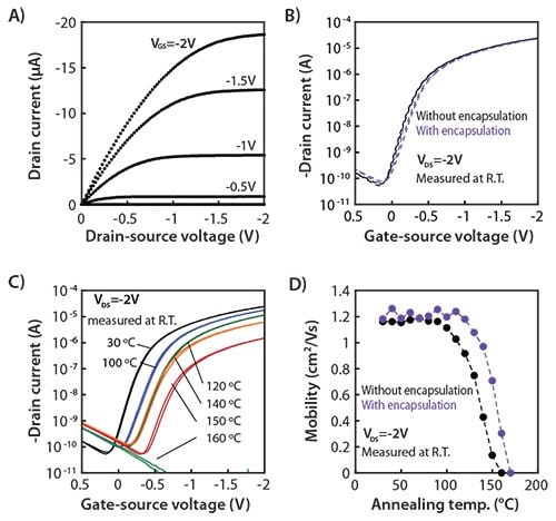
The output and transfer characteristics of the DNTT TFT, measured at 30 °C prior to annealing, are shown in Figures 2A and 2B. The typical mobility is 1.2 cm2/Vs and the on/off ratio exceeds 105 at -2 V operation, indicating excellent TFT characteristics. Performance did not change even after encapsulation (Figure 2B). The effects of annealing were systematically evaluated by comparing the electrical characteristics of the TFTs at 30 °C to the characteristics after annealing at 40 °C for 30 minutes. The devices were then allowed to cool to 30 °C and the characteristics were measured again. The same transistors were then annealed at 50 °C for 30 minutes, cooled to 30 °C, and measured again. This procedure was performed from 30 to 160 °C in temperature increments of 10 °C. All of these experiments were carried out in a nitrogen-filled glove box with less than 1 ppm of oxygen and moisture. Figure 2C shows the transfer characteristics with varying annealing temperatures as measured at room temperature. The on-state drain current (IDS) at gate-source voltage (VGS) = drain-source voltage (VDS) = -2 V decreases slightly upon annealing at 100 °C due to a shift in the threshold voltage toward more negative values. As shown in Figure 2D, the thermal stability of the DNTT TFT with parylene encapsulation is higher than without encapsulation, which is mainly due to high thermal stability of the parylene used. Further annealing above 150 °C results in a degradation of the electrical performance.

Figure 2. Electrical properties of DNTT transistors. A) Output curves of a DNTT TFT before annealing, and B) gate-source voltages (VGS) applied with change from 0 to –2 V in steps of –0.5 V. DC characteristics of a DNTT TFT are measured at room temperature before and after encapsulation. C) DC characteristics of a DNTT TFT measured at room temperature before and after various thermal processes. Transfer curves of a DNTT TFT after annealing in a nitrogen-filled glove box with less than 1 ppm oxygen and moisture at different temperatures. A drain-source voltage (VDS) of –2 V was applied. For each measurement, the TFT was annealed at the indicated temperature and then allowed to cool to 30 °C for the measurement. Annealing temperatures were changed from 40 to 170 °C. D) Mobility as a function of annealing temperature where transistors with and without encapsulation are compared. Measurements are performed in nitrogen gas.20
The effects of annealing at elevated temperatures on the structure of the DNTT films were evaluated by XRD measurements using Cu-Ka X-ray radiation (λ = 1.541 Å).25 The in-plane XRD spectrum of DNTT show three diffraction peaks. A comparison with the X-ray crystallography of singlecrystal DNTT23,27 indicates these three unique peaks correspond to the (110), (020), and (120) lattice planes of DNTT. The diffraction peaks at 2θ = 23° and 27° were found to shift slightly toward larger diffraction angles upon annealing above 100 °C, which corresponds to the temperature beyond which the electrical degradation of the DNTT TFTs begins. From the observed shift of the diffraction peaks, the change of the lattice constants upon annealing can be estimated. In particular, the lattice constant along the a-axis increases by 1.5% from 6.10 to 6.19 Å upon annealing at 160 °C. On the other hand, the lattice constant along the b-axis decreases only slightly by 0.65% from 7.77 to 7.72 Å; whereas, the lattice spacing along the c-axis decreases negligibly by 0.3% from 16.36 to 16.31 Å upon annealing at 160 °C. The observed reduction in the field-effect mobility (from 1.2 to 0.4 cm2/Vs after annealing at 140 °C) is thus attributed to changes induced in the crystal structure of the DNTT film by the following two mechanisms: 1) a phase transition induced at 100 °C that reduces the conductivity within the grains; and 2) a change in the grain shape that reduces the contacts between neighboring grains. The latter mechanism was evidenced from atomic force microscopy (AFM) observations of the DNTT morphology, which revealed that after annealing at 140 °C, the film roughens significantly and features as high as 300 nm begin to emerge.
The thermal stability and electrical performance of gate dielectrics comprising a thin plasma-grown AlOx layer and an alkylphosphonic acid SAM were evaluated from measurements on capacitors consisting of a 20-nm thick Al bottom electrode, a 4-nm thick AlOx layer, a 2-nm thick SAM, and a 50-nm thick Au top electrode. The capacitance of the AlOx/SAM dielectric is stable up to 150 °C; however, it decreases slightly upon annealing at 160 °C (Figure 1E).
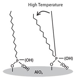
The molecular orientation and stability of the SAM at elevated temperatures were examined using NEXAFS spectroscopy.25,28-30 The integrated intensity of the first angle-dependent s*C-H resonance is evaluated as a function of the X-ray incident angle. The analysis yielded a dichroic ratio (DR) value of 0.5-0.6 for the SAM, suggesting the alkylphosphonic acid molecules within the SAM are oriented with their chains preferentially upright with respect to the substrate; this degree of preferential orientation indicated by the DR is among the highest reported for SAMs. This preferential orientation of the alkylphosphonic acid molecules is maintained up to a temperature of 200 °C, confirming the excellent thermal stability of the SAMs. Analysis with the Building Block Model indicates the molecules within the SAM are tilted with an angle of 13-18° from the surface normal (Figure 3), and this tilt angle is largely preserved upon thermal annealing at elevated temperatures.

Figure 3. Schematic illustration of SAM. The tilt angle of SAM is increased at high temperatures.
Medical Sterilization Procedures on Organic Transistors
Medical sterilization typically involves thermal processes, e.g., heating in an autoclave at 121 °C for 20 minutes with moisture at a pressure of 2 atm or at 150 °C for 20 seconds with moisture at a pressure of 1 atm. The practical applicability of our heat-resistant flexible organic transistors for medical instruments and their ability to simultaneously offer high thermal stability, mechanical flexibility, and sustained electrical performance were demonstrated by subjecting the TFTs to typical sterilization treatments up to 150 °C. We also carried out sterilization at 121 °C for 20 minutes under atmospheric pressure.
The temperature suitability for sterilization was assessed using yeast cells stained with two different dyes: DAPI salt (4′,6-diamidino-2-phenylindole dihydrochloride, D9542), which stains all yeast cells and shows blue fluorescence when excited with UV light; and propidium iodide (P4170), which preferentially stains dead cells and shows red fluorescence when excited with green light. After sterilization at 150 °C for 20 seconds or at 121 °C for 20 minutes in air, the quantification of the fluorescence intensities indicated that 93% of the yeast cells were killed upon sterilization. On the other hand, the on-state drain current (more than 1 μA) and the on/off ratio (8×10⁵) remained practically unaffected by these sterilization procedures.
Flexible Organic Circuits for Medical Catheter
By exploiting the low-temperature processes of the air-stable, heatresistant, organic semiconducting layer and the SAM gate dielectric layer, various substrates can be used for the fabrication of organic transistors, such as rubber,31, 32 conventional polyethylene naphthalate (PEN) with low-Tg,33 and very thin plastic substrates.5
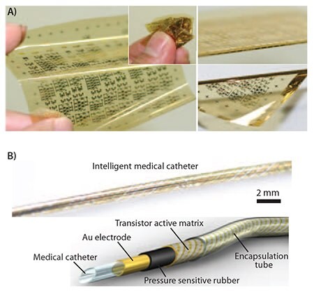
For an electronic application that requires the operation of highperformance circuits folded with an extremely small bending radius, we demonstrated the implementation of organic integrated circuits (ICs) on the inner and outer surfaces of ultrafine rubber tubes with a diameter of 1 mm.5 Due to its novel helical structure and great flexibility, the electrically functionalized tube can bend around turns or corners, and hence, be wrapped around objects. To demonstrate a possible application for organic TFTs operating in the bent state, we manufactured a thin catheter to measure the spatial distribution of mechanical pressure. The sensor was fabricated by laminating three sheets (Figure 4): a foldable 4×36 array of pentacene (698423) TFTs, a pressure-sensitive rubber sheet, and a 12.5-μm thick polyimide sheet with a gold counter electrode. The source contacts of all 144 transistors were connected to the rubber sheet; whereas, the counter electrode was in contact with the opposite surface of the rubber sheet. Upon application of mechanical pressure to the catheter, the electrical resistance between the top and the bottom surfaces of the rubber sheet decreased. A potential of -3 V applied to the counter electrode was supplied to the TFTs at those positions where pressure was applied; thus, the spatial distribution of pressure was obtained by probing the TFTs in the active-matrix array. We believe this approach will lead to various new applications ranging from the functionalization of catheters to artificial blood tubes with pressure sensors. To show the feasibility of the new concept, we also demonstrated the measurement of mechanical pressure using organic transistor-based pressure sensors in this configuration.

Figure 4. Heat-resistant flexible circuit for applications to biomedical electronic devices. A) 12.5-μm-thick polyimide substrate with functional organic TFTs and organic complementary circuits. The array has an area of 75×75 mm2. B) A transistor active-matrix array in the shape of a tightly wound helix. An ultraflexible active-matrix pressure sensor array as a concept of a catheter that measures the spatial distribution of pressure along its length and circumference by means of an active-matrix sensor helix.5
Conclusions and Future Prospects
Heat-resistant, flexible, organic thin-film transistors have been demonstrated to withstand the harsh conditions of medical sterilization procedures. One of the most attractive features of flexible electronics is their biocompatibility. In addition to wearable electronics including sensors and actuators that operate outside the body, implantable electronics that function inside the body are expected to play important roles in healthcare. For example, flexible pressure and thermal sensors can realize electrically powered artificial skin, and flexible vibration and photodetectors can work as an electrically powered artificial auris interna and retina, respectively. Given their excellent mechanical flexibility and softness, users might implant those with the lower resistance to electronic objects in the body. Furthermore, if the flexible organic circuits are comprised of biocompatible materials, electronic implants can be used inside the body without fear of immune rejection.
Apart from their applications in healthcare, flexible electronics should find applications in electronic devices that are used in daily life. For example, flexible organic circuits fabricated on banknotes can be used as an ultimate anticounterfeit technology and tracking system. Organic ICs with exceptional flexibility and bending stability can realize new concepts in electronics and open up human-friendly electronic systems.
Acknowledgments
This study was partially supported by KAKENHI (Wakate S & Wakate A), and the Special Coordination Funds for Promoting and Technology. We thank Dr. He Wang, Prof. Yueh-Lin Loo (Princeton University), Dr. Cherno Jaye, Dr. Daniel Fischer (National Institute of Standards and Technology) for the NEXAFS measurements and discussion; Dr. Hagen Klauk, Dr. Ute Zschieschang (Max Planck Institute for Solid State Research) for the SAM technology; and Dr. Tatsuya Yamamoto, Prof. Kazuo Takimiya (Hiroshima University), Dr. Masaaki Ikeda, Hirokazu Kuwabara (Nippon Kayaku Co., Ltd.) for DNTT, Prof. Takayasu Sakurai, and Prof. Makoto Takamiya (University of Tokyo) for the circuit design. We also thank Dojindo Molecular Technologies Inc. for the high-purity fluorescent dye and Daisankasei Co., Ltd., for the high-purity parylene (diX-SR).
Materials
References
To continue reading please sign in or create an account.
Don't Have An Account?