The Role of Alkanethiols in Interfacial Engineering
Self-assembled monolayers (SAMs) enable precise atomic control over solid-state interfaces, but achieving defect-free execution requires absolute chemical purity. Trace contaminants cause competitive adsorption, which disrupts molecular lattices and degrades thin-film device performance.
Surface-engineering materials are used to support the development of reproducible device architectures:
- High-purity linear alkanethiols (≥98-99% Assay) engineered for defect-free crystalline assemblies;
- Target-specific interfacial anchors (≥97% Assay), including functionalized, branched, and multi-dentate phosphonic or silane precursors optimized for diverse substrate geometries; and
- Scalable industrial passivation agents (≥95% Purum) deployed for robust macro-scale moisture and oxidation barriers. SAM materials are used in thin-film fabrication to support the study and optimization of interfacial properties.
Monolayer architecture and surface chemistry
SAMs are organized molecular assemblies that form spontaneously, either from solution or gas-phase adsorption, directly onto a solid substrate.1 Among these, alkanethiol SAMs stand out for their structural stability and immense versatility. Typically formed by the adsorption of n-alkanethiolate molecules onto noble-metal substrates such as gold, silver, or palladium, they offer precise control over key surface properties including hydrophobicity and chemical reactivity.1,2
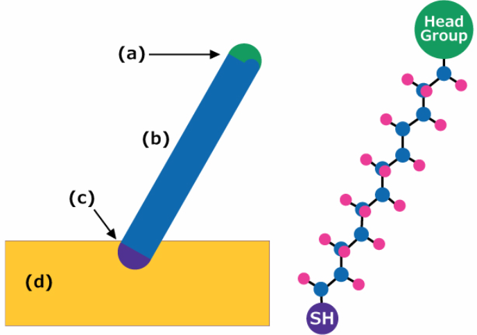
Figure 1.Generalized structure of an alkanethiol self-assembled monolayer (SAM), highlighting (a) the terminal head group, (b) the alkyl spacer chain, (c) the sulfur anchoring group that binds to the substrate, and (d) the substrate surface.
The physical and electronic properties of alkanethiol SAMs are critically governed by chain length, which determines packing density, molecular tilt angle, dielectric thickness, and tunnelling barrier height.3,4 As illustrated in Figure 1, a typical C12 alkanethiol consists of a surface-binding sulfur anchor, an alkyl chain, and a terminal head group whose structure influences monolayer organization and interfacial properties. Achieving a well-ordered monolayer requires a minimum alkane chain of 10-carbons (C10). This length represents the precise thermodynamic threshold at which hydrophobic inter-chain van der Waals interactions become strong enough to overcome the molecules’ rotational degrees of freedom, locking molecules into a stable lattice.4,5
Researchers can custom-design surfaces with molecular-level control to achieve targeted functions, from biosensing and electronics to corrosion protection. This precision is unlocked by tailoring the terminal head group of the self-assembling molecule. The exposed chemical group directly dictates how the functionalized surface interacts with its macro-environment, as detailed in Table 1.1,6,7
Thermodynamics and assembly kinetics
SAMs are typically formed by incubating a substrate in a dilute (~1 mM) alkanethiol solution using ethanol as the primary solvent.2 While initial monolayer coverage occurs rapidly through chemisorption within seconds to minutes,6 this early phase yields a highly disorganized “lying down” phase riddled with gauche defects.8 Full structural ordering, dense packing, and the transition to a “standing up” orientation develops gradually. This phase transition requires anywhere from 12 hours to 2 days as the molecule maximize their intermolecular packing.5,8
Because monolayer crystallization relies on thermodynamic error-correction, sourcing precursors engineered to stringent purity thresholds (>=98-99% assay) is critical. This level of purity eliminates short-chain thiols or oxidized disulfides that cause competitive adsorption, phase-separated lattice defects, and electronic trap states. This heavily impacts (PEGₙ) thiol monolayers: trace carboxylic acid-terminated contaminants disrupt the neutral hydration layer, accelerating non-specific protein adsorption and rendering the resulting surface more fouling than bare gold itself.6
To ensure physical thin-film execution successfully replicates predictive machine learning (ML) and high-throughput screening (HTS) packing simulations, device engineers must specify high-grade precursors that eliminate gauche defects and maintain work-function alignment.9
Interfacial engineering in thin film electronics
Advanced thin-film device design
Interfacial engineering is a key strategy for advancing thin-film device performance across organic electronics, perovskites, and hybrid systems. It underpins the development of solution-processed devices, including organic field-effect transistors (OFETs), organic solar cells (OSCs), perovskite solar cells (PVSCs), and organic light-emitting diodes (OLEDs). Historically, commercial progress was constrained by stability, mechanical flexibility, and electronic trap-state limitations of bulky, conventional interfacial materials.
SAMs provide an alternative approach to addressing these limitations. They present a combination of interfacial properties:
- Optical Transparency - Ultrathin, single-molecule geometry eliminates parasitic optical absorption across active spectra.
- Chemical diversity - Near-unlimited head group tunability allows precise work-function matching7
- Robustness - Stable chemisorption via strong Au-S or Ag-S bonds ensures long-term mechanical and thermal integrity1,2
- Sensor capability & Selectivity - Highly sensitive surface functionalization allows precise control over surface-molecule interactions10
- Surface passivation - Effective reduction of electronic trap-state density at semiconductor-electrode interfaces11
This versatility has driven rapid SAM adoption across a broad application landscape -extending from solar cells and microarray substrates to atomic layer deposition (ALD) blocking layers in organic thin-film transistors (OTFTs).7, 11-14
SAM integration in perovskite solar cells
SAMs serve four critical functions at perovskite solar cells’s (PVSCs) interface: energy level alignment between the transport layer and perovskite absorber, perovskite film morphology improvement, defect-state passivation at electrode interfaces, and work function tuning of transparent conductive electrodes (ITO, FTO). Their appeal is equally practical: SAMs offer minimal light absorption, low material consumption, straightforward deposition, and conformal coating. Together, these properties enable PVSCs to achieve gains in efficiency and stability through reduced interfacial defects, enhanced charge extraction, and improved resistance to moisture and oxygen.11
The inverted (p-i-n) architecture has become the standard configuration for SAM-based perovskite solar cells, favored for its superior stability and natural compatibility with bottom-up SAM deposition. In this geometry, the SAM is deposited directly at the ITO/perovskite interface, replacing conventional and bulkier, hole transport layers (such as PEDOT:PSS or nickel oxide) with a molecularly thin, highly functional alternative.11
Technical Note: While noble-metal contacts rely on sulfur chemisorption,1,2 hydroxyl-rich metal oxide interfaces (ITO/FTO) in high-efficiency p-i-n perovskite solar cells require specialized carbazole-based and phosphonic acid SAM precursors, such as [2-(9H-carbazol-9-yl)ethyl]phosphonic acid (2PACz), and Octadecylphosphonic acid (97%), to ensure robust covalent anchoring.7
Complementing these rigid oxide anchors, modern p-i-n layouts leverage branched Tier 2 surface modifiers like 2-Ethylhexanethiol (97%) directly at active interfaces; its unique side-chain branching alters the molecular tilt angle to optimize energy level alignment and promote uniform perovskite film crystallization.
Neuromorphic electronics and synapses
Beyond traditional photovoltaics, specialized SAM architectures are driving innovations in next-generation neuromorphic computing. Photonic synapses hold significant promise for robotics and artificial intelligence applications. Highly crystalline, conjugated benzo-naphthol-thiophene SAMs integrated into the semiconducting channel of biomimetic photosynapses deliver a compelling combination of synaptic functionalities: paired-pulse facilitation, ultralow energy consumption, and both short- and long-term plasticity .15 These crystalline SAMs, with their diverse charge trap sites, also enable UV protection and human-like learning behavior, positioning them as a compelling materials platform for next-generation neuromorphic devices.15
SAM barriers in biosensing and microarrays
Long-chain alkanethiol SAMs form densely packed, well-ordered films that create a membrane-like microenvironment ideally suited for biomolecule immobilization.10 Their reproducible formation on noble-metal substrates (Au, Ag) enables stable electrochemical, optical, and piezoelectric transducer measurements while maintaining chemical specificity after coupling.2,10 Furthermore, their structural tunability provides molecular-level insights into protein adsorption, DNA hybridization, and antigen-antibody interactions via surface-sensitive techniques like AFM and STM.10
For electronic applications, thermally deposited gold functionalized with n-alkanethiol SAMs (C3, C6, C8, and longer) serves as an insulating interface in electrolyte-gated OFETs (EG-OFETs). These monolayers passivate the electrode surface and suppress unwanted Faradaic reactions to stabilize device operation. Specifically, 1-Hexanethiol, 1-Octanethiol SAMs form highly ordered, superior crystalline barriers that prevent device metric saturation for up to ~25 operating cycles, whereas short propanethiol layers exhibit severe pinhole defects resembling bare gold with significantly poorer long-term passivation.9
For specialized array architectures, mixed alkanethiol SAMs, frequently incorporating matrices like 1-Hexadecanethiol alongside a 35% 1-Undecanethiol and 65% 11-Mercapto-1-undecanol blend, enable precise surface wetting control. These mixed layers deliver spatially homogeneous surface characteristics across substrates, remaining stable when stored at 4 °C for up to 6 months.13 To achieve intermediate packing densities and tailor molecular-level friction across electronic interfaces, high-purity mid-chain derivatives such as 1-Nonanethiol provide an optimized spatial footprint that ensures precise local crystalline order.2,10
Case study: An Octadecanethiol (ODT)-based SAM on a gold surface, further modified with 1-fluoro-2-nitro-4-azidobenzene (FNAB) and cholesterol oxidase (ChOx), functions as a bioelectrode for cholesterol detection by surface plasmon resonance (SPR). The resulting sensor delivers a linear response across 50-500 mg/dL, with a detection limit of 50 mg/dL and a storage shelf life of approximately 2 months at 4 °C.16
Industrial anti-corrosion protection and ALD blocking
Because densely packed alkanethiol SAMs form impermeable molecular barriers, their utility extends to industrial metallization and surface protection. For instance, 1-Dodecanethiol SAMs deployed on cobalt substrates provide effective protection against oxidation and corrosion, making them highly relevant across catalysis, magnetic recording media, pigments, and medical implant applications. When deposition parameters are optimized-including surface pre-treatment protocols, ethanol solvent parameters, and substrate immersion times-the resulting crystalline monolayer is densely packed and stable, preventing metal reoxidation for up to 28 days in open air.
In semiconductor processing, alkanethiol SAMs on copper and gold offer a cost-effective, low-defect alternative for selective ALD blocking layers. High-purity linear compounds like 1-Decanethiol, 11-Mercaptoundecanoic acid, and 1-Tetradecanethiol are particularly effective at inhibiting material growth during sequential gas-surface reactions. Furthermore, 1-Decanethiol is widely employed for asymmetric electrode functionalization in OTFTs, enabling precise charge injection control across solar cells, photodetectors, and sensor arrays.
While these highly precise lithographic and electronic lines require strict analytical-grade linear tracks to eliminate molecular leakage, scalable industrial operations successfully deploy cost-effective Tier 3 bulk barriers like 1-Octadecanethiol (purum). This grade functions as an ideal material for applications where high-volume processing demands macro-scale moisture insulation, general oxidation protection, and reliable copper passivation across high-density chip architectures.