Block Copolymers in Nanoscale Patterning
Introduction
For more than a decade, block copolymers have garnered significant interest as self-assembling materials for nanoscale patterning.1 This interest stems from the propensity of block copolymers to assemble into distinct, nanometer-sized domains that exhibit ordered morphologies at equilibrium.2 In thin films (<100 nm), these morphologies, which are typically lamellar, cylindrical, or spherical in nature, can form ordered arrays of lines or spots with feature dimensions of 5–50 nm. These ordered arrays can serve as templates for nanoscale patterning and other technological applications. Typically, one block of the copolymer is removed, and the remaining material serves as a soft etch mask. Block copolymer material systems that have been used in this context include polystyrene-block-polybutadiene ((PS-b-PB), with the polybutadiene selectively removed by ozone),1 PS-block-polylactide (polylactide selectively chemically degraded),3 PS-block-polydimethylsiloxane (PS selectively removed by reactive ion etching (RIE)),4 and PS-blockpolyferrocenyldialkylsilane systems (PS selectively removed by RIE).5
By far, the most common block copolymer that researchers have used in the study of nanoscale patterning is polystyrene-block-poly(methyl methacrylate) (PS-b-PMMA). The PMMA domains can be selectively removed by UV exposure,6 and the remaining material can serve as templates for etching the underlying substrate.7 PS-b-PMMA also has the advantage that the surface energies of PS and PMMA at the annealing temperature (190–230 °C) are remarkably similar.8 Because of this similarity in surface energies, there is not a strong driving force for either block to reside at the surface of the film, and morphological patterns can go all the way through the film. Research with PS-b-PMMA has shown that the diameter of cylindrical domains can be selected to be 14–50 nm, depending on the molecular weight (Mn) of the block copolymer.9 Addition of PS and PMMA homopolymer to the PS-b- PMMA to form a blend can also affect the diameter of the cylinders, resulting in diameters and domain spacings that are anywhere from 10% smaller to 150% larger than the corresponding values of the pure PS-b-PMMA, depending on the relative amount and Mn of the homopolymers added to the block copolymer.6
Self-assembled Arrays of Block Copolymer Domains
For pattern formation by assembled block copolymers domains, lines can be made either by lamellae that are perpendicular to the substrate, or by cylinders that are parallel to the substrate, and spots can be made by spheres or by cylinders that are perpendicular to the substrate. One advantage of PS-b-PMMA is that high aspect ratio, perpendicular domains can be achieved, which are preferable for pattern transfer. To assemble perpendicular structures, it is typically necessary to control the wetting interactions of the polymer on the surface,8 the thickness of the film,10 and the annealing temperature.11,12 A standard method to chemically modify the surface to control the wetting interactions for PS-b-PMMA comes from the seminal work of Mansky et al., who grafted random copolymer brushes comprised of styrene and methyl methacrylate (P(S-r-MMA)) onto silicon substrates.8 With the appropriate fraction of styrene (FSt) in the P(S-r-MMA), the P(S-r-MMA) is nonpreferential to wetting by either block of the PS-b-PMMA. P(S-r-MMA) can be easily synthesized via a combination of functional monomer and initiator, as outlined in Figure 1. Hydroxyl terminated polymer brushes can be synthesized from nitroxide-mediated polymerization (NMP) using functional initiators bearing a free hydroxyl group (Figure 1a).13,14 Copolymers capable of grafting to native oxide surfaces or forming cross-linked mats via their side chain functionality can be achieved by either NMP or free radical polymerization techniques.13,14 These materials are then easily used to form a non-preferential brush on the surface by dehydration or forming a cross-linked insoluble mat (Method 1 in Figure 1b). Alternatively, non-preferential surfaces can be achieved by exposure of octadecyl-trichlorosilane self-assembled monolayers (SAMs) to X-ray irradiation where the exposure dose defines the wetting characteristics of the SAM (Method 2 in Figure 1b).15,16 For either method, once the substrate is treated to make it non-preferential, a block copolymer film is spin-coated onto the substrate, and then annealed so that it can assemble into its equilibrium morphology.
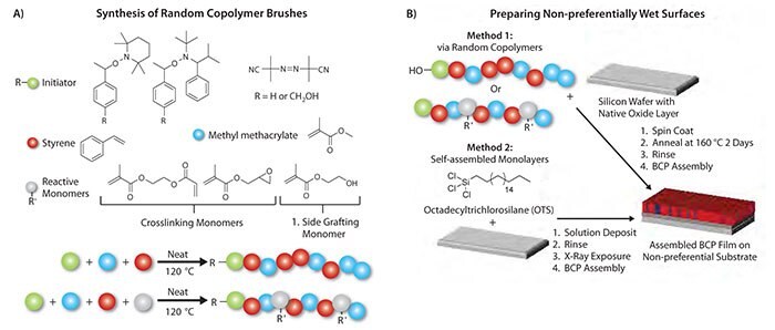
Figure 1. Synthesis of random copolymers (A) and the two methods of preparation of non-preferential surfaces (B). Non-preferential surfaces are formed by either spin coating and annealing random copolymers (Method 1), or forming a self-assembled monolayer and exposing to x-rays (Method 2). After preparation of the non-preferential surface, a block copolymer (BCP) can be spin coated onto the surface, and then annealed to achieve its equilibrium morphology.
The FSt that is appropriate for use as a non-preferential surface treatment depends on the morphology of the PS-b-PMMA to be assembled on the random copolymer brush or mat. In the case of the self-assembly of lamellae-forming PS-b-PMMA, a random copolymer of styrene and methyl methacrylate (P(S-r-MMA)) must have FSt in the range of 0.45–0.78 to be non-preferential to the assembled PS-b-PMMA.8,13,17 In contrast, the non-preferential FSt range for PS-b-PMMA that forms PS or PMMA cylinders is 0.55–0.57 or 0.59–0.72, respectively, as shown in the scanning electron microscope (SEM) images in Figure 2.13 The thickness of the PS-b-PMMA film also plays an important role in the assembly of perpendicular domains that span the film thickness. Perpendicular domains can be readily achieved when the film thickness is 13–40 nm.17 For thicker films (up to 300 nm), precise control of FSt and annealing temperature is required to achieve perpendicularly-oriented domains.11 Porous films of block copolymer formed by the removal of the polymer in the cylindrical domains have been employed as a template for a host of applications, including the fabrication of MOSFET′s,18 quantum dots,19,20 high surface area capacitors,21 photovoltaic devices,22 porous membranes,23 magnetic nanowires,24 and bit patterned media.25
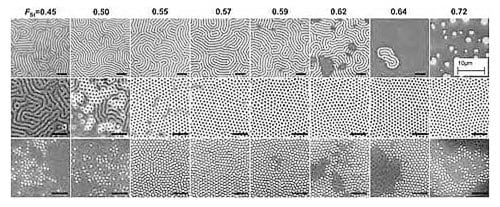
Figure 2. Effect of mole fraction of styrene (FSt) in a P(S-r-MMA) brush on the orientation of self-assembled films of PS-b-PMMA. The rows of top-down SEM images correspond to lamellae forming (top), PMMA cylinder forming (middle), and PS cylinder forming (bottom) PS-b-PMMA. Black scale bars correspond to 200 nm. Reprinted with permission from ACS.
Directed Assembly of Block Copolymer Domains
Self-assembly of block copolymer domains has several technological applications and is of great scientific interest. However, some applications, such as bit patterned media and integrated circuits,27 require control over the location and geometry of the assembled domains. Directed assembly with a chemical pattern provides a robust method of ordering the domains in a way that allows them to be registered to features on the underlying substrate. The directed assembly process starts with the formation of a lithographically defined chemical pattern. An example of a directed assembly process flow from previous work is shown in the left-most process flow in Figure 3.28 In this process, a PS brush is uniformly grafted on a silicon wafer. The PS brush is then coated with a photoresist, which is subsequently lithographically patterned and developed. The substrate is then treated with an oxygen plasma, such that the exposed portions of the PS brush are oxidized. Removal of the remaining photoresist yields a chemical pattern in which the areas of the PS brush that were exposed to the oxygen plasma are preferentially wet in the PMMA block of PS-b-PMMA, and unexposed areas are preferentially wet in the PS block. Once the chemical pattern is formed, a thin film of PS-b-PMMA is spin coated on top of it, and then annealed. During annealing, the block copolymer equilibrates in the presence of the chemical pattern, and the preferential wetting of the different regions of the pattern directs the assembly of the domains of the PS-b-PMMA, as shown in the SEMs in Figure 3 (for cylinders) and Figure 4 (for lamellae).
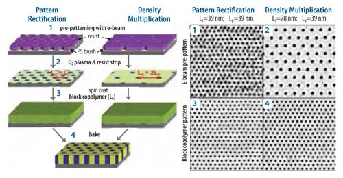
Figure 3. On the left is shown a schematic of the chemical pattern fabrication process for the directed assembly of cylinder-forming PS-b-PMMA, for both with (right) and without (left) density multiplication. 1-2) SEM images of the patterned photoresist. 3-4) SEM images of the block copolymer film on top of prepattern defined by the corresponding pattern above.
It is also possible to make the chemical pattern using a cross-linked polymer brush as the starting material, as shown in the schematic in Figure 4.29 The use of a cross-linked mat offers several advantages. First, it permits the use of a trim etch, so that the dimensions of the pattern features, such as the pattern line width W, can be finely controlled. Second, it dissociates the chemistry of the pattern features from the chemistry of the rest of the pattern. For example, in the schematic in Figure 4, the red guiding lines of the chemical pattern are cross-linked PS, and the rest of the chemical pattern is a P(S-r-MMA) brush, with a composition tailored specifically for directed assembly. Finally, because of the high cross-link density of the PS guiding lines, the chemistry of the cross-linked PS is unaffected by the photoresist patterning process and chemicals, and is therefore more robust.
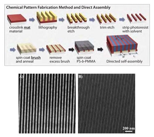
Figure 4. Schematic of the chemical pattern fabrication process for density multiplication using lamellae forming PS-b-PMMA. (Reprinted with permission from ACS.29) A) SEM image of the patterned photoresist (period = 80 nm), B) SEM image of the blockcopolymer film (period = 40 nm) on top of the pattern in A).
Recent work has shown that chemical patterns can direct the assembly of block copolymers such that the density of features on the top surface of the assembled block copolymer is an integer multiple of the density of features on the chemical pattern.7,30 The initial research on directed assembly focused on a 1:1 match of the assembled domains and the features of the chemical pattern, such as that shown in the left-most schematic in Figure 3, and in the SEMs in Figure 3a and Figure 3c.31,32 While 1:1 directed assembly offers many potential advantages for advanced lithography related to uniformity of feature size and shape,33,34 the ability to assemble block copolymers with a greater feature density than is on the chemical pattern is highly desired and would allow for increased resolution over current lithographic systems. General process schematics for directed assembly with density multiplication are shown on the right in Figure 3 (cylinders), at the top of Figure 4 (lamellae), and on the left in Figure 5 (more complicated, device-oriented structures). In each case, the spacing of the features of the chemical pattern, Ls, is approximately equal to an integer multiple of the spacing of the domains in the bulk block copolymer, L0. When the block copolymer domains assemble, the domains of a specific block of the copolymer will be registered to the guiding lines of the chemical pattern, and the same type of domains must assemble interpolated between guiding lines. As a result of directed assembly with density multiplication, the PS-b-PMMA cylinders in Figure 3d have a fourfold higher density than the patterned spots of the chemical pattern in Figure 3b that was used to direct the assembly. Similarly, the PS-b-PMMA lamellae in Figure 4b have a two-fold higher density than the cross-linked PS guiding lines in the chemical pattern in Figure 4a.
The alternating brightness and darkness of the assembled PS domains in Figure 4b is evidence of the cross-linked PS and the P(S-r-MMA) brush, respectively, of the chemical pattern underlying the assembled PS-b-PMMA.
Directed assembly with density multiplication is also shown in the SEMs in Figure 5, but in this case the assembled structures demonstrate another important capability of directed assembly of block copolymers: the ability to assemble into device-oriented structures.35 While there are useful applications of naturally-occurring structures such as parallel lines and hexagonal arrays of spots, for many applications of advanced lithography it is necessary for more complex geometries, such as line segments, 90º bends, jogs, T-junctions, periodic arrays of spots, and isolated lines and spots.36 Earlier research has shown the ability to direct the assembly of block copolymers on the chemical patterns to form each of these structures without density multiplication.34,37 Recent research has shown that many of these features can also be assembled with density multiplication, as shown in the bends, jogs, T-junctions, and line terminations shown in the SEMs in Figure 5.35
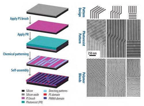
Figure 5. On the left is shown a schematic of the directed assembly process for the directed assembly of a block copolymer into device-oriented geometries with density multiplication. On the right is shown the chemical pattern design (top row), SEM images of the photoresist pattern (middle row), and the corresponding block copolymerhomopolymer ternary blends (bottom row) directed to assemble into device-oriented structures.35
Conclusion
The understanding and application of directed assembly has made huge gains over the past decade, but there are still many opportunity for research and innovation. For example, the bulk of the research on directed assembly, including the work described above, has been done with PS-b-PMMA. While significant advancements have been made, it is reasonable to assume that for some applications it would be beneficial to use other block copolymer systems, such as organometallic or siliconcontaining block copolymers. Similarly, it may be valuable to use block copolymer systems that can assemble into smaller domain structures than PS-b-PMMA. Thus, directed assembly of block copolymers remains a rich field of exploration, both for new scientific discoveries and technological implementation of our current knowledge of the process.
References
To continue reading please sign in or create an account.
Don't Have An Account?