Advancements in Organic Electronics
Article Sections
- Introduction
- Realization of Integrated Circuits Using Organic Thin-Film Transistors
- High-Performance Fully Solution-Processed Organic Integrated Circuits Using a Pseudo-CMOS Circuit Configuration
- Ultra-Low Voltage Drive Organic Integrated Circuit Using a Parylene Dielectric Layer
- Complementary Integrated Circuits Employing Printed OTFTs With Stacked Structures
- Complementary Integrated Circuits Employing SAM Electrode Surface Modification For n-Type Semiconductors
- Complementary Integrated Circuits Using Finely-Patterned Electrodes Formed by Reverse Offset Printing
- Conclusion
- Funding Sources
- Acknowledgments
Introduction
Electronics based on organic semiconductor materials are called organic electronics. Typical applications are organic transistors, organic light-emitting diodes, and organic solar cells. Compared to conventional approaches, organic electronics are lightweight, flexible, and thinner, enabling applications such as flexible displays, large-area, lightweight solar cells, electronic skins, and the like.
The reasons why these advantages are realized are as follows. Since an organic semiconductor can be processed at low temperatures, thin-film layers can be formed on plastic film substrates with low-heat resistance such as polyethylenenaphthalate (PEN, GF23662043, GF58055766). Furthermore, it is possible to fabricate electronic devices using printing techniques by creating inks that employ soluble semiconductor materials. Fabricating an electronic device using printing techniques instead of vacuum process provides for electronic devices that are scalable over large areas, drastically reducing production costs.
We will focus on organic thin-film transistors (OTFT) in this review. The performance and solubility of the organic semiconductors used in OTFTs are improving year by year. Carrier mobility is a primary semiconductor performance metric, and many materials have exhibited values of 10 cm2/Vs or more, exceeding that of amorphous silicon (a-Si) TFT devices.
Most research on OTFT devices has focused on the various aspects of organic semiconductor materials, gate insulator materials, electrode formation methods, device structures, surface treatments, and applications for integrated circuits. In this paper, we will share insights gained through the development of the fabrication processes for OTFT devices and their integrated circuits, and report on the results gained from evaluation of their electrical characteristics.
Realization of integrated circuits using organic thin-film transistors
Our research group has not only developed advanced semiconductor materials for OTFT device fabrication, but we have also extensively researched OTFT device architectures and integrated circuits and carried out new application development.
Fabricating OTFT devices using printing technologies is one way to take advantage of the benefit of organic electronic devices, and we are also optimizing and newly developing the printing processes employed. Here, the fabricating methods and electrical characteristics of OTFT-based integrated circuits are described.
High-performance fully solution-processed organic integrated circuits using a pseudo- CMOS circuit configuration
P-type semiconductors generally exhibit higher performance than n-type semiconductors, in properties such as carrier mobility and atmospheric stability. This is because the deep work function (W.F.) of commonly used gold or silver electrode materials align well with the highest occupied molecular orbital (HOMO)/lowest unoccupied molecular orbital (LUMO) level of the p-type semiconductor. Also, due to their low ionization potential, p-type semiconductors exhibit minimal deterioration due to moisture and oxygen.
On the other hand, n-type semiconductors are known to have lower atmospheric stability and carrier mobility than p-type semiconductors. Therefore, if an integrated circuit can be configured using only p-type OTFT devices, high-performance integrated circuits can generally be realized. The research described in this section is a pseudo-CMOS1 (Complementary Metal Oxide Semiconductor)integrated circuit composed of p-type OTFT fabricated by either solution-based or printing processes.
The procedure of the OTFT fabrication process using fully solution-based or printing methods is as follows:
To form an electrode using the inkjet printing method, the surface state of the substrate on which the ink lands is important such that the wettability must be controlled by the base layer. In this case, a cross-linked PVP using melamine as a cross-linking agent was used as a base layer, upon which a gate electrode was formed.
Water-based solvent silver nanoparticle (SNP) ink (DIC, JAGLT- 01) was used as the gate electrode material. Since water-based solvent ink is less susceptible to the coffee ring effect than hydrocarbon-based solvent inks, we used it for application to a gate electrode that requires high flatness in a bottom-gate bottom-contact (BGBC) structure (Figure 1B).
Next, a cross-linked PVP (Poly(4-vinylphenol)) film was used to form a gate dielectric layer by spin-coating. SNP ink (900190, 901975, 901971) and a hydrocarbon-based solvent were used to form source and drain electrodes by inkjet printing.
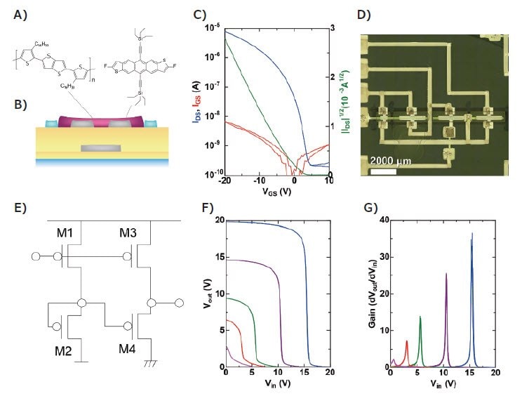
Figure 1. A) Chemical structure of the p-type organic semiconductor material. The left side shows the polymer semiconductor, pBTTT-C16, and the right side shows low molecular semiconductor, diF-TES-ADT. B) Cross-sectional image of the fully printed or solution-processed organic thin-film transistor, which has a BGBC structure used in this section. C) Transfer characteristics and D) microscope image of the fabricated OTFT device. E) Circuit diagram of pseudo-CMOS circuit and F) input / output characteristics and G) gain characteristics of the fabricated pseudo-CMOS inverter circuit.
Then, a hydrophobic polymer bank (AF1600X, DuPont) was formed around the source/drain electrodes by a dispenser system (Imaging Master 350PC, Musashi Engineering, Inc.) in order to define an area for semiconductor printing. Finally, an organic semiconductor ink in which pBTTT-C16 (Figure 1A-left) is dissolved in o-dichlorobenzene (240664) was printed by a dispenser system.
In this fabricating process, various treatment processes such as sintering and annealing are added after each step. The temperature is kept at 150 °C or lower during each step to enable fabrication on a flexible plastic substrate such as PEN. Figure 1C shows the transistor characteristics of the fully solution/printing processed OTFT. The fabricated OTFT operated with good performance at an operating voltage of 20 V, mobility of 0.03 cm2/Vs, threshold voltage (Vth) of -1.2 V, and on/off current ratio of 104.
We applied a pseudo-CMOS circuit configuration to construct an inverter circuit as the basis for an integrated circuit. The highperformance pseudo-CMOS inverter circuit can be configured using only p-type OTFTs. Figure 1D shows a microscopic image of the fabricated pseudo-CMOS circuit, and Figure 1E shows a circuit diagram. Figure 1F–G show the input-output and gain characteristics for a pseudo-CMOS inverter circuit using the fabricated OTFT devices. Operating began from a supply voltage of 5 V, and a gain of 34 was obtained at 20 V, excellent performance values for a fully solution-processed type inverter circuit. Using the same processes, basic gates of digital circuits such as NAND (Negative AND) and NOR (Negative OR) circuits were fabricated and also showed good performance.1
The OTFT device performance was further improved by applying a self-assembled monolayer (SAM) surface treatment to the source/drain electrode surfaces and using a small molecule solution (diF-TES-ADT, 754099), as shown in Figure 1A-right for the p-type semiconductor. As a result, we succeeded in fabricating a high-performance flip-flop (FF) circuit with the pseudo-CMOS configuration.2
Ultra-low voltage drive organic integrated circuit using a parylene dielectric layer
To improve the carrier mobility, it is necessary to optimize device fabrication conditions or to employ semiconductor materials with inherently high mobility. We further improved the performance of the OTFT device by changing the semiconductor materials, using polymer blends, and applying it to amplifier circuits.
In recent years, research reports on small molecular semiconductor materials with high mobility of 10 cm2/Vs or more such as C8-2,7-diocytyl[1]benzothieno[3,2-b][1] benzothiophene (C8- BTBT, 747092) and C10-dinaptho[2,3-b:2’,3’-f]thieno[3,2-b]thiophene (C10- DNTT) have increased. We fabricated an OTFT device using a smallmolecule, p-type semiconductor material ditheino[2’3-d,3’d’]- benzo[1,2,-b:4,-b’]-dithiophene (DTBDT)-C6 (Tosoh Corporation) that exhibits high mobility.4
When a polymer dielectric is mixed with a small-molecule semiconductor material, it is converted into an ink. The layers are separated during the drying process to form a good dielectric /semiconductor interface. In this case, polystyrene (PS) was selected for the polymer dielectric, and an optimized blend of concentrations was used.
The device structure of the fabricated OTFT device is shown in Figure 2A, and the transfer characteristics of the transistor are shown in Figure 2B. The device showed high performance, operated at an extremely low voltage of 2 V or less, a mobility of 1.1 cm2/Vs, a threshold voltage of -0.26 V, and a subthreshold slope (SS) value of 100 mV/dec. This very low SS value is generally realized from low-level trap states, and this study suggests that there are few trap levels at the semiconductor/ polymer interface.5
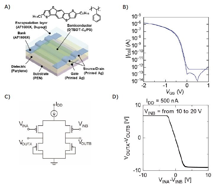
Figure 2. A). Schematic of the device structure for the fabricated low-voltage operation OTFT device and B) its transfer characteristics. C) The circuit diagram of the fabricated differential amplifier and D) its input/output characteristics.
Next, the high-performance OTFT device using DTBDT-C6 (dithieno[2,3-d;2’,3’-d’]benzo-[1,2-b;4,5-b’]dithiophene) was used to apply to an operational amplification circuit for biosensors.6 DTBDT-C6 is known for very little variation in electrical characteristics, so a key feature of OTFT devices using DTBCT-C6 is small performance variations. Variations in OTFT devices cause a deviation in electrical characteristics, resulting in malfunctions when an integrated circuit is constructed. An OTFT device fabricated using DTBDT-C6 had an average mobility of 1.1 ± 0.17 cm2/Vs and a threshold voltage of -0.01 ± 0.09 V, which is relatively high mobility and very small variations.
An operational amplifier circuit was fabricated using this lowvariation OTFT device. The circuit diagram of the fabricated differential amplifier circuit is shown in Figure 2C, and typical input/output characteristics are shown in Figure 2D. This is a circuit that amplifies the difference between two input signals, and it is required to match the OTFT device characteristics with high accuracy. Since the fabricated organic thin-film transistors are characterized by high uniformity, a functioning operational amplifier circuit was realized.
Complementary integrated circuits employing printed OTFTs with stacked structures
Complementary integrated circuits require p-type and n-type OTFT devices and are expected to have higher switching performance and improved power savings than p-metal oxidesemiconductor (pMOS) and n-type metal-oxide semiconductor (nMOS) circuits using either p-type or n-type TFT device. Therefore, a complementary integrated circuit is most suitable for electronic devices that are expected to be driven by a battery, solar cell, or bio-battery, such as wearables.
In collaboration with Ube Industries, we have developed a small molecule n-type semiconductor called TU-3 that has high atmospheric stability and high mobility (911135). We used this n-type semiconductor to fabricate a complementary integrated circuit with a stacked structure. This approach not only improves the degree of circuit integration7 but also aims to form an appropriate SAM surface treatment on each of the source/drain electrodes of the p-type and n-type OTFT devices.8
In general, an electrode material having a deep work function is most suitable for a p-type semiconductor, and a shallow electrode material is most suitable for an n-type semiconductor. Pentafluorobenzenethiol (PFBT) has been reported as a selfassembled monolayer (SAM) surface treatment material for p-type semiconductors, and 4-Methylbenzenethiol (4-MBT, T28525) and Polyethylenimine (PEI, 306185 ) have been reported for n-type semiconductors.
Since immersion and spin-coating methods are generally used to form the SAM surface treatment layer, it is necessary to expose only the source/drain electrodes of the p-type/n-type OTFT or to remove the unnecessary portions after formation. Therefore, we applied a stacked structure and formed source/drain electrodes for the p-type and n-type OTFT devices in separate layers. Since the immersion method and spin-coating method are generally used as a method for forming the SAM surface treatment layer, it is necessary to expose only the source/drain electrodes of the p-type/n-type OTFT devices or to remove unnecessary portions after formation. Therefore, we employed a stacked structure and formed source/drain electrodes for the p-type and n-type OTFT devices in separate layers.
As a result, we succeeded in SAM layer formation suitable for each semiconductor using the simple immersion method. At the same time, we succeeded in increasing the degree of integration by 2 and 3 times by increasing the number of layers.9 Figure 3A shows the cross-sectional structure of the fabricated complementary integrated circuit. A photograph of the device fabricated on a 12.5 cm square glass substrate is shown in Figure 3B. The fabricated integrated circuit, a p-type OTFT device having a bottom-gate bottom-contact (BGBC) construction is formed on an n-type OTFT device having a topgate bottom-contact (TGBC) construction.
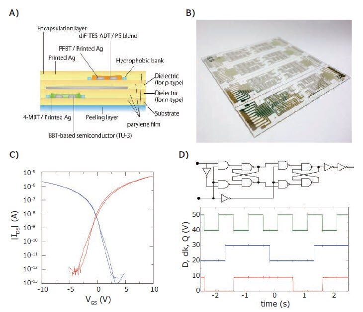
Figure 3. A). Schematic of the device structure for a complementary integrated circuit having a stacked structure and B) a photograph of devices fabricated on a 125 mm square glass substrate. C) Transfer characteristics of the fabricated p-type and n-type OTFT devices and a circuit diagram and input/output characteristics of a D-FF circuit.
The fabricated p-type and n-type OTFT devices each exhibited good performance. The p-type OTFT device using 2,8-difluoro- 5,11-bis(triethylsilyethynyl)anthradithiophene (diF-TES-ADT) for the semiconductor layer showed a mobility of 0.34 cm2/Vs, a threshold voltage of 0.2 V, and an on/off ratio of 107 at an operating voltage of 10 V. The n-type OTFT device using TU-3 were 0.29 cm2/Vs, 2.0 V, and 107, respectively (Figure 3C). Figure 3D showed the results of fabricating D-type Flip-Flop (D-FF) circuit using these OTFT devices and the evaluated circuit characteristics. The fabricated D-FF circuit worked normally and proved the feasibility of the created integrated circuits using printing processes.
Complementary integrated circuits employing SAM electrode surface modification for n-type semiconductors
A major drawback of complementary integrated circuits using stacked structures is an increase in the number of processing steps. Therefore, by using p-type semiconductors that do not require a SAM surface treatment, we formed source/drain electrodes of p-type and n-type OTFT on the same plane to simplify processing. This semiconductor material employed is characterized by a wide process window that includes highheat resistance and a variety of printing methods. When this semiconductor is used, a complementary integrated circuit can be fabricated similarly to the fabricating process of a single OTFT device. First, after forming a parylene base layer on a glass substrate, SNP ink was used to form the source/drain electrode by an inkjet printing method. After that, SAM surface treatment material for n-type semiconductor is formed on all source/drain electrodes (Figure 4A).
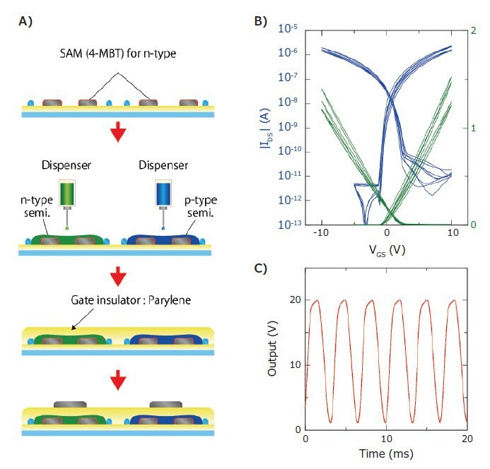
Figure 4. A) Illustration of the manufacturing process steps. B) Transfer characteristics of the fabricated OTFT device. C) Oscillation signal of the fabricated ring oscillator circuit when operating at 20 V.
Next, a p-type semiconductor (MOP-01, Mitsubishi Chemical) and an n-type semiconductor (TU-3, FIC) are printed using a dispenser system. Afterwards, they are annealed at 150 °C for 30 minutes. After forming the parylene as the gate insulating film, a gate electrode is formed under the same conditions as the source/drain electrodes, and a complementary integrated circuit was fabricated.10 Before forming the gate electrode, a hole was made in the gate dielectric using a YAG (Yttrium Aluminum Garnet) laser system.
The fabricated p-type and n-type OTFT devices each demonstrated good electrical characteristics. As a demonstration of the fabricated complementary integrated circuit, we formed an array of 10×10 ring oscillators on a glass substrate. The fabricated p-type and n-type organic OTFT devices had mobilities of 0.11 and 0.19 cm2/Vs, threshold voltages of 0.09 V and 1.40 V, and on/off current ratios of 105 and 107, respectively (Figure 4B). One-hundred (100) ring oscillators were fabricated and were shown to operate well at a drive voltage of 1 V, and the propagation delay time per stage at 20 V was 0.34 ms (Figure 4C). The fabrication yield obtained for the ring oscillators was 100%.
Complementary integrated circuits using finely-patterned electrodes formed by reverse offset printing
It is difficult to miniaturize electrodes formed by the inkjet printing method, and the line width and line interval are limited. For example, electrodes formed with inkjet nozzles widely used in printed electrode research (10 pL) have electrode widths of 100 to 200 μm and line spacing (channel length: L) of 10 μm or more. Therefore, we have focused on the reversal offset printing (ROP) method and have succeeded in using it in forming fine electrodes.11 Figure 5A shows the process step diagram for reverse offset printing. It consists of three steps: coating, patterning, and transfer. Therefore, an integrated circuit with finely patterned electrodes can be realized by combining this ROP method with a complementary integrated circuit fabricated process using a stacked structure. The manufacturing process used was the same as that used electrodes formed using the inkjet printing method.
The complementary integrated circuit that was formed had an electrode width of 15 μm, a line spacing of 10 μm, and a line width of about one-tenth of that of an inkjet-printed electrode. Silver nanoparticle ink (RO100GE, Future Ink Corporation) was used for electrode formation with a sintering temperature of 120 °C. The variations in line spacing in the source/drain electrode patterns were less than ±1 μm, with a line spacing target value of 2.5 to 70 μm. Figure 5B shows a microscopic image of an electrode with a width of 15μm and a line spacing of 2.5 μm. These results show that the patterning reproducibility and printing accuracy are very high. Figure 5C shows the input/ output characteristics of the fabricated inverter circuit. Since it was found to have good electrical performance when driven from 2.5 V to 10 V,12 it was employed to a ring oscillator circuit.
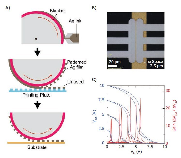
Figure 5. A) A schematic diagram of the printing steps for reverse offset printing and B) a printed silver electrode with a line width of 15 μm and a line spacing of 2.5 μm. C) Input/output characteristics of a complementary inverter circuit fabricated with finely patterned electrodes.
The characteristics of the fabricated ring oscillator circuit are ten-times higher than that of a complementary integrated circuit fabricated by using the inkjet printing method, which is the result of a shortened-channel OTFT device and reduced overlap area.
Conclusion
We have developed fabrication processes for OTFT devices and integrated circuits using printing and solution-processing techniques. We first focused on pseudo-CMOS circuits using only p-type OTFT devices, demonstrated inverter circuits and flip-flop circuits, and evaluated the circuit operation.
In the next stage, we achieved high-mobility, low-voltage drive, and uniform characteristics using high-performance small molecule semiconductors and succeeded in fabricating ultralow- voltage operating inverter circuits and differential amplifier circuits. We demonstrated the feasibility of amplifier circuits by employing it in biosensor signal amplification.
Finally, we developed two complementary integrated circuit fabrication processes consisting of p-type and n-type OTFT devices. One process employs a fabrication process in which the source/drain electrode layers of p-type / n-type OTFT devices are separated using a stacked structure, and the electrode surface modification is realized using a simple immersion method. The other fabrication process forms p-type and n-type OTFT devices on the same plane using p-type semiconductors that exhibit high performance on various electrode surfaces. As a result, we successfully realized a complementary, integrated circuit with a small number of process steps as compared with the fabrication process using the stacked structure.
At present, many challenges remain for improving OTFT device performance and miniaturization. In the future, overcoming these issues will help to realize next-generation electronic devices such as high-performance wearable computers.
Funding Sources
JST COI Grant Number JPMJCE1312, and JSPS KAKENHI (Early-Career Scientists) Grant Numbers 18K13797.
Acknowledgments
This work was partially supported by JST COI Grant Number JPMJCE1312, and JSPS KAKENHI (Early-Career Scientists) Grant Numbers 18K13797. We thank Tosoh Corporation for supplying DTBDT-C6 and Mitsubishi Chemical Corporation for supplying MOP-01.
Materials
References
To continue reading please sign in or create an account.
Don't Have An Account?