Scalable Fabrication of Organic Electronic Devices Using SAMs
Introduction
This article focuses on the use of self-assembled monolayers (SAMs) to support the transition of organic thin-film transistor (OTFT) fabrication from laboratory-scale development to reproducible pilot and pilot-line manufacturing. Scaling OTFT fabrication from lab to pilot manufacturing requires controlling device-to-device variability across production batches. Charge transport occurs chiefly at two interfaces, the dielectric-semiconductor interface and the electrode-semiconductor interface, whose interfacial energetics and morphology are sensitive to processing conditions. SAMs, including silane-based and alkanethiol-based systems, modify surface energy and trap-state density to promote reproducible device performance. This article presents a workflow-driven framework that links device architecture, material selection, interface engineering, and processing constraints. Structured decision matrices support systematic evaluation of material systems at each fabrication stage.
End-to-end workflow
Organic electronic device fabrication involves a sequence of interdependent steps, where material selection, interface modification, and processing conditions influence overall device behavior. The following sections describe key workflow stages, linking device requirements to compatible material systems, and fabrication constraints.
Device architecture and performance parameters
In Organic Field-Effect Transistors (OFETs), uniform device performance depends on control of thin-film crystallinity, interface trap state density, and device configuration. In small-molecule organic semiconductors, charge transport is sensitive to molecular packing and grain size due to weak intermolecular interactions. Variations in film morphology during deposition can contribute to device-to-device variability across production batches.
Charge-carrier mobility is influenced by two electrical interfaces that are present across all common device architectures:
- The Dielectric-Semiconductor Interface governs charge accumulation and localized trap state density.
- The Electrode-Semiconductor Interface governs contact resistance and charge injection characteristics.
Device architecture selection (Bottom-Gate Bottom-Contact [BGBC], Bottom-Gate Top-Contact [BGTC], or top-gate) is the first workflow step, followed by interface engineering using SAMs and silanes. These choices influence semiconductor thin-film morphology and charge transport characteristics.
SAMs modify interfacial energetics at both interface regions. Silane-based SAMs, including Trichloro(octadecyl)silane (C18-OTS, 104817) and (3-Glycidyloxypropyl)trimethoxysilane (GPTMS, 440167), deposit onto dielectric surfaces, reducing trap state density and promoting thin-film ordering. Alkanethiol SAMs, including 1-octanethiol (471836) and 1-dodecanethiol (471364), modify metal electrode work function and adjust energy level alignment at the electrode-semiconductor interface.
Device architecture, interface chemistry, and material properties are evaluated together, as each parameter influences charge transport behavior within the completed device structure. The four standard OTFT device configurations are illustrated in Figure 1. Each architecture defines a distinct positional relationship between gate electrode, dielectric, SAM, semiconductor, and contacts, with direct implications for the processing sequence and interface engineering strategy.
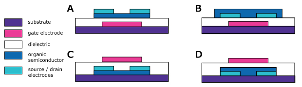
Figure 1.Four standard OFET device configurations: (a) Bottom-Gate Bottom-Contact (BGBC), (b) Bottom-Gate Top-Contact (BGTC), (c) Top-Gate Bottom-Contact, (d) Top-Gate Top-Contact. In bottom-gate (BG) architectures, silane SAMs are applied to the dielectric surface to reduce trap states; in bottom-contact (BC) architectures, thiol SAMs are applied to metal electrodes to tune work function.
Selection of organic semiconductor materials
The selection of an organic semiconductor material determines the manufacturing approach, processing method compatibility, and expected electrical characteristics for the device. Material properties, including molecular structure, energy levels, and solubility, each constrain the available fabrication routes.
Table 1 presents a selection matrix relating target device applications and material constraints to compatible processing methods and representative semiconductor material classes. The semiconductor material selected at this stage establishes the processing conditions for subsequent interface and dielectric engineering steps.
Following selection of the semiconductor material and associated processing approach, the next stage involves evaluation of interfacial and dielectric properties within the device structure.
Interface and dielectric considerations
In OFETs, charge transport occurs mostly within the first few nanometers of the semiconductor layer adjacent to the dielectric surface. Consequently, the dielectric-semiconductor and electrode-semiconductor interface regions directly affect device-to-device reproducibility and electrical characteristics, including operating voltage and charge transport behavior.
Table 2 summarizes the relationship between electrical constraints, interface chemistry requirements, and representative material classes used in device fabrication. Interface and dielectric material selection at this stage determines gate dielectric capacitance, interfacial trap state density, and the electrostatic boundary conditions that govern subsequent fabrication steps.
Table 2. Interface & dielectric selection matrix
Stable interface and dielectric properties define the boundary conditions for subsequent fabrication steps, including assessment of processing compatibility and selection of orthogonal material systems.
Processing compatibility and orthogonal systems
Fabrication of high-density organic circuitry requires patterning methods compatible with the chemical and thermal stability limits of organic thin films. To prevent damage to organic layers during standard photolithographic processes, surface-chemistry methods, including the selective deposition of SAMs, define substrate features while minimizing solvent or plasma exposure.
Table 3 summarizes the relationships between patterning resolution requirements, substrate and process constraints, and SAM-based material systems applicable to device feature definition.
Table 3. Patterning & device definition matrix: SAM material selection & resolution control
Defined spatial patterning and interface modification establish the structural framework for subsequent fabrication steps, including multilayer processing and material compatibility considerations.
Device integration
Integrated circuit fabrication demands precise material handling and process control across multiple steps to maintain electrical and structural integrity. Table 4 summarizes the relationships between device architecture requirements, integration constraints, and representative material systems used in multilayer organic electronic device fabrication.
Table 4. Device integration matrix: multilayer co-optimization & high-purity circuitry
Coordination of material compatibility and processing conditions during device integration defines the baseline electrical characteristics of the system and informs subsequent optimization of device performance.
Performance optimization
OTFT performance depends on interdependent parameters, and the three primary parameters subject to material level control are:
- Carrier Mobility: Charge transport is influenced by semiconductor crystallinity and trap state density at the dielectric interface. Larger crystal grain domains and lower interfacial trap density correlate with higher charge-carrier mobility. SAM-passivated gate dielectrics reduce trap state density at the dielectric-semiconductor interface.
- Threshold Voltage (Vth): Channel charge accumulation depends on gate dielectric capacitance and interfacial dipole formation. Threshold voltage can be tuned by modifying dielectric layer properties or incorporating interfacial dipolar layers between the gate dielectric and semiconductor.
- Operational Stability: Bias stress, ambient gas exposure, and interfacial degradation are factors that can introduce hysteresis and shift electrical characteristics over time. Encapsulation and chemically stable interfacial layers limit these effects.
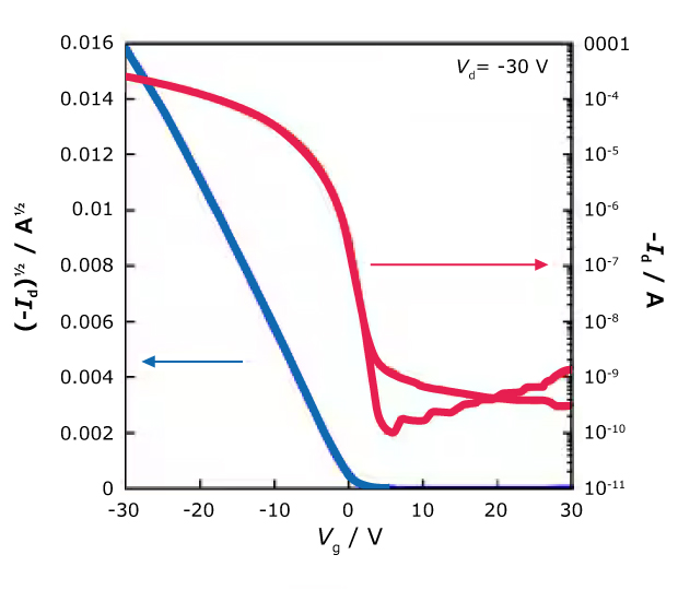
Figure 2.Typical transfer characteristics of the DNTT-based OFET devices fabricated on Si/SiO2 substrate.
Transfer characteristics for dinaphtho[2,3-b:2',3'-f]thieno[3,2-b]thiophene (DNTT)-based OFETs with C18-OTS (104817) SAM dielectric treatment appear in Figure 2.1 The curves confirm the low off-current, minimal hysteresis, and sharp subthreshold turn-on characteristic of a well-ordered SAM–dielectric interface, establishing reliable benchmarks for the mobility and threshold voltage metrics discussed in this section.
Figure 3 shows representative transfer IV curves for devices #3 and #5 from a set of seven triple-sublimed pentacene OFETs on crystalline OTS (104817, 442291) SAM-treated SiO₂. Across the seven devices, on/off ratios exceeded 10⁶ and the average hole mobility was 3.4 cm²/V·s, demonstrating that combining high-purity semiconductor material with a well-ordered crystalline SAM dielectric surface yields significant reproducibility gains. The key transistor metrics (mobility, on/off and threshold voltage) for seven OTFTs fabricated using Triple-Sublimed Pentacene are given in Table 5.
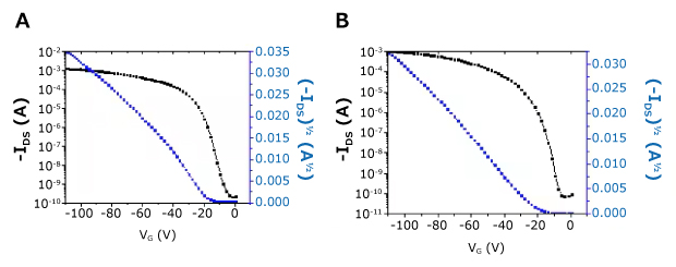
Figure 3. Transfer IV curves for triple-sublimed pentacene OFETs (Device #3 left; Device #5 right) on a crystalline octadecylsilane (OTS) dielectric SAM/SiO₂. On/off >10⁶; average mobility 3.4 cm²/Vs (max 4.6); drain-source voltage (V_DS) = −100 V.
Application integration
The final stage of the fabrication workflow aligns device architecture with the intended operating environment. At this stage, the workflow maps application requirements to device-level mechanisms, material selection, and performance characteristics. Table 6 maps end-use applications to underlying electronic mechanisms and representative material classes used in organic electronic devices.
Table 6. Application selection matrix: SAM-enabled material architectures
Conclusion
Transitioning organic electronic devices from laboratory-scale development to scalable fabrication involves coordination of material selection, interface engineering, and processing conditions. Parameters such as semiconductor properties, surface modification using SAMs, solvent compatibility, and low-temperature deposition methods influence device reproducibility and performance. A workflow-based approach enables systematic evaluation of these factors, improving consistency across fabrication steps, and supporting the development of organic electronic devices for flexible and transparent applications.