Photopatterning Self-Assembled Monolayers
Self-assembled monolayers (SAMs) have attracted enormous interest for a wide variety of applications in micro- and nano-technology.
In this article, we compare the benefits of three different classes of SAM systems (alkylthiolates on gold, alkylsilanes on silicon dioxide and alkylphosphonic acids on oxide surfaces), and illustrate how photopatterning techniques can be used to fabricate structures with sizes from 10 nm upwards over areas ranging from a few microns to square centimeters in size. Self-assembled monolayers1-3 have become indispensible tools in many areas of nanoscience. A SAM is isostructural with a Langmuir-Blodgett (LB) film – it consists of a close-packed, ordered layer of molecular adsorbates on a solid surface – but unlike an LB film, it is deposited in a simple process involving immersion of a substrate in a dilute solution of the adsorbate. The monolayer assembly process is driven by the formation of a strong specific interaction between the adsorbate and substrate, but intermolecular interactions significantly enhance stability and drive ordering. Although the term “self-assembled monolayer” is often used loosely, to refer to almost any organic adsorbate system, strictly speaking a SAM has the following features: (a) a monolayer of amphiphilic molecules adsorbed on a solid surface; (b) a strong (usually chemisorption) adsorbate-substrate interaction; (c) close-packing; and, usually, (d) a high degree of order.
Alkylthiolate SAMs
SAMs of alkythiolates on gold are formed by immersion of a gold film, formed on a suitable substrate, into a dilute (1 mMol) ethanolic solution of the appropriate adsorbate. They exhibit excellent chemical stability and a high degree of order (in 5–10 nm domains, they are effectively crystalline), because of the strength of the Au−S interaction, the similarity in the spacing between adsorption sites (4.99 Å) and the van der Waals diameter of an alkyl chain (4.5 Å). Alklythiolates also form SAMs on a variety of other metals (Ag, Cu and Pd have been widely studied) and some semiconductors (e.g., GaAs).
The principal limitations on the use of alkylthiolate SAMs arise from their modest thermal and oxidative stability: alkylthiolates desorb from surfaces at temperatures not much higher than room temperature, making many types of solution-phase processing difficult; and they exhibit a high susceptibility to ambient oxidation, most likely due to atmospheric ozone, which attacks the S−Au bond. Often, for example in biology, a low density of defects introduced by partial oxidative degradation may lead to a significant impairment of performance. Finally, the requirement to use a gold substrate is also a limitation. For example, gold has a propensity to quench fluorescence, a problem where optical characterization of adsorbed biomolecules is required.
The most widely used patterning technique for alkylthiolate SAMs is microcontact printing (μCP),4 originally developed by Whitesides and co-workers as an inexpensive alternative to conventional microfabrication methods. In μCP, a poly(dimethylsiloxane) (PDMS) stamp is inked with a solution of a thiol and placed on a gold substrate, facilitating thiol transfer. Regions not coated in the initial step may be functionalized with a second thiol in a solution-phase deposition step. μCP has been very widely used because it offers a rapid, inexpensive and highly effective means of patterning monolayers on sub-micrometer length scales. At the nanometer scale, dip-pen nanolithography (DPN)5 presents a nanoscopic analogue of μCP. An atomic force microscope (AFM) tip is inked in the appropriate thiol solution, and used to trace features across a surface. DPN offers a resolution significantly better than 100 nm for alkylthiolate inks, and a variety of highly sophisticated adaptations of the technique have been reported, including parallel writing devices.6
An alternate route is the photopatterning of alkylthiolate SAMs by exposure to UV light through a mask (Figure 1a).7 This causes photooxidation of the adsorbate to yield a sulfonate species, which is only weakly adsorbed and may be displaced in a simple solution-phase process. An advantage of this approach is that the first-formed SAM exhibits a very high degree of order. Illumination at ca. 250 nm is required, to initiate hot electron formation leading to SAM photooxidation. While many mercury lamps emit at this wavelength, their emission spectra depend quite strongly on the nature of the source. The best approach is to use a UV laser (e.g. a frequency-doubled argon ion laser). At the nanometer scale, a scanning near-field optical microscope may be coupled to a UV laser and used to carry out exposure of the SAM (Figure 1b).8 For complete photo-oxidation of the SAM, an exposure of ~1-4 J cm-2 is required, depending on tail group and chain length. Subsequently, photo-oxidized adsorbates may be replaced in a solution-phase process. In this approach, called scanning near-field photolithography, structures as small as 9 nm may be fabricated.9
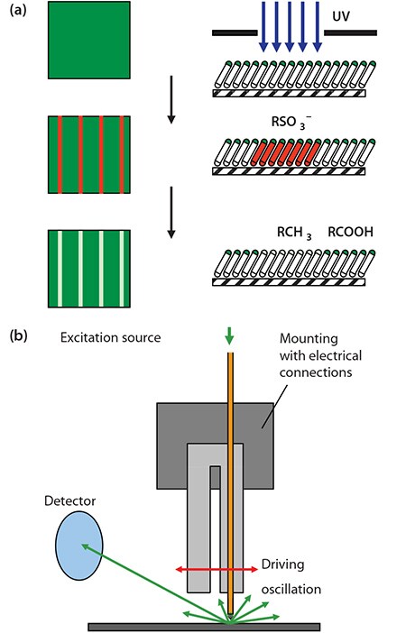
Figure 1. a) Schematic diagram showing the photopatterning of a SAM of alkylthiolates on gold. b) In scanning near-field photolithography, a near-field probe is utilized to carry out exposure with a resolution that may be as good as 9 nm (ca. λ/30).
Alkylsilane SAMs
Alkoxysilanes and trichlorosilanes react with silanol groups at silica surfaces to yield strongly bound films with exceptional oxidative and thermal stability. The biggest experimental challenge is to control polymerization between adsorbates, typically driven by the presence of too much water in the organic solvent in which the silane is typically dissolved. Polymerization can lead to the formation of rough, globular deposits. Often, silane films are thicker than a monolayer, and they typically exhibit lower degrees of ordering than alkylthiolate SAMs. In many applications, the enhanced thermal and oxidative stability and the capacity for functionalization of glass are attractive and justify the use of the more complex preparation routes. At the nanometer scale, Sagiv and co-workers have demonstrated that using an AFM with a bias voltage applied to the probe, alkylsilane SAMs may be selectively oxidized and re-functionalized with contrasting adsorbates, thus facilitating the construction of complex molecular structures.10
Alkylphosphonate SAMs
Oxide surfaces are important for many applications. For example, in the dye-sensitized solar cell, nanostructured Ti oxides are used to optimize the interfacial area and maximize electronic transfer from the dye to the semiconductor.11 Alkylphosphonic acids (APA) adsorb strongly onto the oxides of aluminum, titanium and other metals to form SAMs that are closer packed and exhibit greater oxidative and thermal stability than do alkylthiolate monolayers. APA SAMs are stable during long periods of atmospheric exposure. Degradation is only a significant issue on extended exposure to aqueous conditions.
SAMs on Aluminum Oxide
The monolayer is formed by a simple solution-phase deposition process, involving immersion of the substrate in a dilute solution of APA in a suitable solvent (e.g. ethanol). The substrate, usually sputtered or evaporated Al, must be exposed to the ambient atmosphere for 20 to 40 minutes to allow the surface to become hydroxylated. During SAM formation, the APA head group is thought to be deprotonated, and interacts strongly with the oxide surface. The spacing between head groups is slightly smaller (4.8 Å) than is the case in alkylthiolate SAMs. Vibrational spectroscopy indicates that the numbers of gauche defects are extremely small, indicating that the adsorbates adopt a highly ordered all-trans conformation. Alkylphosphonate SAMs offer enormous promise for many applications, and are perhaps the most underexploited of the SAM systems.
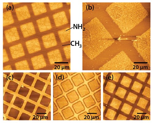
Figure 2. a) Pattern of squares of aminobutylphosphonic acid (Prod. No. A0664) formed in an octadecylphosphonic acid (Prod. No 715166) SAM on aluminum oxide by photolithography. Following exposure of the methyl terminated SAM through a mask, the sample was immersed in a solution of the amine functionalized adsorbate to re-functionalize the degraded regions. b) A similar sample to the one shown in (a) following attachment of aldehyde-functionalized polymer nanoparticles. c) – e): photopatterned octadecylphosphonic acid SAMs following UV exposure and subsequent etching in sodium hydroxide. Exposures / J cm-2: (a) 10, (b) 10, (c) 2, (d) 20, and (e) 40.
Compared to alkylthiolate SAMs, very little work has been done on the patterning of APA monolayers. However, photopatterning offers a simple approach.12 On exposure to UV light with a wavelength of ca. 250 nm, the P-C bond in the adsorbate is cleaved, leading to removal of the alkyl tail. The phosphonate group is thought to remain at the surface, but this does not prevent the re-functionalization of the modified region by a second, contrasting APA. The result is a pattern of different chemical composition. Figure 2a shows an image of a pattern created in an APA SAM by photolithography. A mask was placed over a monolayer of octadecylphosphonic acid (ODPA, Prod. No. 715166), and the sample was exposed to UV light. After exposure, the mask was removed and the sample immersed in an aqueous solution of aminobutylphosphonic acid (ABPA, Prod. No. A0664). The sample was imaged by friction force microscopy (FFM), a form of atomic force microscopy in which lateral deflections of the cantilever, determined by surface friction, are measured, so that the hydrophilic regions exhibit bright contrast (i.e., increased friction). Figure 2b shows a similar sample following attachment of aldehyde-functionalized polymer nanoparticles, via imine bond formation, illustrating that such approaches form a simple, effective means of building up more complex molecular structures on oxide surfaces.
Alternatively, after the UV exposure, the patterned ODPA layer may be used as a resist to etch structures into the underlying Al film. Figure 2c shows a sample exposed to 2 J cm−2 of irradiation at 244 nm. On immersion in a solution of sodium hydroxide, the exposed areas (squares) were etched, leaving the regions covered by intact adsorbates unmodified. APA SAMs behave as “switchable resists”, where increasing the UV exposure gradually modifies the behavior (perhaps through remodeling of the oxide in the exposed areas) such that at an exposure of 40 J cm−2 (Figure 2e) the patterned SAM effectively behaves as a negative tone resist, with etching being fastest in regions masked during exposure. Exposure of the APA SAM using a near-field probe enables the fabrication of nanostructures by wet chemical etching. Figure 3 shows two images of a series of lines that have been formed by scanning near-field photolithography (SNP). The line width is ca. 100 nm. The principal limitation on resolution appears to be the rather large grain size of the Al film as better results have been obtained previously for gold films.
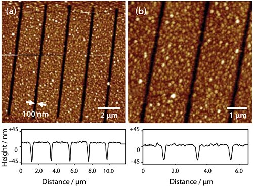
Figure 3. Tapping mode AFM images of nanostructures formed by using SNP-patterned phosphonic acid monolayers as resists for the etching of Al.
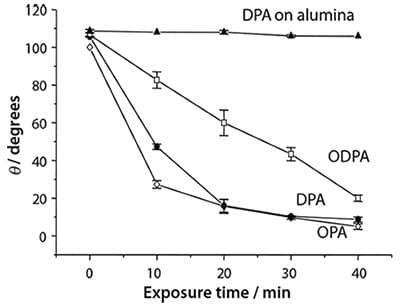
Figure 4. The variation in the contact angle with the immersion time in water for SAMs of octyl- (OPA), decyl- (DPA) and octadecyl phosphonic acids (ODPA) on the native oxide of titanium, and for DPA on alumina.
SAMs on Titanium Oxide
Titania exhibits a well-documented photocatalytic effect: absorption of UV light creates electron-hole pairs at the oxide surface leading to the oxidative breakdown of organic matter. This enables the rapid photopatterning of APA on Ti.13 Figure 4 shows contact angle data for a variety of SAMs on titania, and for monolayers of decyl phosphonic acid (DPA) on alumina. Following UV exposure, degradation of the alkyl chain exposes the underlying polar oxide surface and causes a decrease in the contact angle. It is clear that the rate of change is much faster on titania: even the longest adsorbate, ODPA, is degraded much faster than a SAM of DPA on alumina. Longer wavelengths are also useable for SAMs on titania than is the case on alumina; provided the photon energy is greater than the titania band gap, oxidation will occur. Shorter wavelengths are necessary on alumina because direct scission of a C-P bond is the initial step in the process.
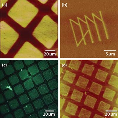
Figure 5. a) FFM image of an ODPA SAM on the native oxide of titanium following exposure through a mask (600 mesh) at 50 mW for 2 min (7.5 J cm-2). Z-scale range: 0 – 517 mV. b) FFM image of a pattern produced in an ODPA monolayer on titanium oxide using scanning near-field photolithography. z-scale range: 0 – 1.00 V. c) Fluorescence microscopy image of a similar sample to that shown in (a) but where the exposed areas have been functionalized first with ABPA and then, subsequently, with aldehyde-functionalized polymer nanoparticles loaded with a fluorescent dye. d) A sample that has been etched in sodium hydroxide following exposure of an ODPA SAM.
Figure 5a shows an FFM image of a SAM of ODPA following UV exposure through a mask. The exposed regions (squares) exhibit bright contrast because the underlying substrate has been exposed, yielding a localized increase in the surface free energy that causes an increase in the coefficient of friction. Figure 5b shows a pattern fabricated using the same UV degradation chemistry, but with a near field probe as the light source. The functionalization of patterned SAMs on titania is demonstrated in the optical micrograph in Figure 5c, which shows a fluorescence emitted from aldhehyde-functionalized, dye-loaded polymer nanoparticles coupled to ABPA adsorbed into oxide regions exposed by photopatterning. Finally, Figure 5d shows a sample that has been patterned by exposure of an ODPA SAM followed by solutionphase etching with potassium hydroxide. Similar kind of exposuredependent switchable character has been reported for SAMs on Ti. The nature of the behavior is also dependent on the etch solution: a sample prepared in exactly the same way to that shown in Figure 5d but etched with piranha solution yielded inverted contrast (i.e., the patterned SAM appeared to exhibit positive tone character, as opposed to the negative tone character shown).
Conclusions
Self-assembled monolayers of alkyl phosphonic acids are underexploited in nanoscience. They exhibit extremely good oxidative stability, and can be readily patterned using photolithographic techniques. A wide range of functionalization strategies is accessible, via simple replacement of photodegradaed adsorbates or by wet etching of patterned monolayers. The photocatalytic degradation of SAMs on titania enables the rapid patterning of SAMs over a broad range of wavelengths.
Materials
Materials
References
如要继续阅读,请登录或创建帐户。
暂无帐户?