Silylethyne-substituted Pentacenes
Introduction
Research into the use of organic semiconductors in field-effect transistors (FETs) began in earnest in the mid-1990s,1 after early exciting results from vapor-deposited small molecule semiconductors.2 The drive for low-cost processing capabilities then led to significant advances in polymeric semiconductors, which offered lower performance but simplified fabrication.3 More recently, soluble small-molecule systems are providing the high performance of vapor deposited systems with the convenience of low-cost solution-based processing techniques.4 The earliest soluble small molecule approaches involved the reversible solubilization of highperformance chromophores such as pentacene or oligothiophenes.5 A current approach to soluble materials relies on functionalization of linearly-fused chromophores with substituents that take advantage of both steric and π-stacking interactions to induce these chromophores to self-assemble into arrays with strong intermolecular electronic coupling.6 The resulting highly engineered materials offer simple processing from solution to yield robust electronic devices. The strong tendency for these materials to self-assemble yields uniform fields with significant longrange crystalline order, which leads to field-effect transistor devices with performance that rivals, and in some cases surpasses, the performance of vapor-deposited small molecules.
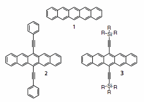
Figure 1.Pentacene (1), phenylethynyl pentacene (2) and silylethynyl pentacenes (3).
Of the linearly-fused compounds, pentacene (Product No. 698423) is perhaps the most exhaustively studied, and is considered a “benchmark” organic semiconductor.7 It is not surprising that this chromophore has also been the subject of numerous functionalization studies, in attempts to improve the stability and solubility of the material.8 One of the most versatile pentacene substituent classes is the trialkylsilyl alkyne. Silylethyne substitution offers excellent opportunity to tune solubility for application-specific needs and self-assembly for electronic performance, and has yielded semiconductors with excellent device performance.
Synthesis
Ethyne-substituted pentacenes in general have been known since the 1960s, when phenylethynyl derivatives (2) were proposed as red emitters in chemiluminescent systems.9 Although these materials are generally poorly soluble, recently, one phenylethyne derivative has shown reasonable mobility in top-contact devices.10 More versatile are the trialkylsilylethynyl derivatives.11 The synthesis of these compounds (Scheme 1) follows the same basic procedure as the phenylethyne derivatives, namely addition of an alkyne anion to commerciallyavailable pentacenequinone (Product No. 246883) followed by deoxygenation using either HI (Product No. 210013) or SnCl2 (Product No. 452335).12,13 It has recently been shown that a mixture of KI (Product No. 60399) and NaH2PO2 (Product No. S8282) in acetic acid (Product No. 338826) is the preferred reagent in cases where the pentacene unit contains strongly electron-withdrawing groups.14 For use in electronic devices, the purity of the resulting materials is critical - even small amounts of impurities can lead to poor film crystallinity, decreased material stability and dismal electronic performance.15 Because of the highly non-polar nature of these molecules and the typical impurities, the separation of byproducts is often problematic. Thus, the successful synthesis relies heavily on the purity of starting materials.
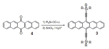
Scheme 1.Ethynylpentacene synthesis.
Crystal Packing
The formation of crystalline films of soluble pentacenes is critical, since the electronic properties of the films evolves from the crystalline arrangement of the individual molecule, and the close-packed arrangement of molecules yields significantly improved stability over amorphous films.16 The crystal packing of silylethyne-substituted pentacenes is conveniently tuned by changing the alkyl substituents on silicon.11 A number of examples of the crystal motifs accessible are shown in Figure 2. For the tert-butyldimethylsilyl (3a), triethylsilyl (3b), triisopropylsilyl (3c), and tris(trimethylsilyl)silyl (3d) derivatives shown in the Figure 2, we see that crystal packing can be shifted between onedimensional columnar stacks, one-dimensional slipped stacks, twodimensional stacks and purely edge-to-face interactions.
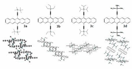
Figure 2.Representative silylethyne pentacene derivatives and their crystal packing.
Intrinsic Properties
For planar devices (such as FETs), we have found that materials with two-dimensional π-stacking interactions yield the most uniform films and provide the best device performance. Of these, the 6,13-bis(triisopropylsilylethynyl) pentacene derivative (TIPS pentacene 3c (Product No. 716006)) has proven to be quite successful for applications in organic electronics and is the most intensively studied soluble pentacene. Band structure calculations on a variety of silylethyne-substituted pentacenes show significant dispersion in both the conduction and valence bands, predicting significant potential for high hole and electron mobility.17 This potential was confirmed by optical pump-THz probe studies on single crystals of TIPS pentacene 3c and triethylsilyl derivative 3b, showing that both materials exhibit mobilities of the same order as that of unsubstituted pentacene.18
OFETs
Device applications of this class of compounds were first reported in 2003, with the analysis of vapor-deposited films of a series of silylethyne-functionalized pentacenes in bottom-contact transistors.19 A key finding of these studies was the need to heat the device substrates to over 85°C during deposition in order to achieve suitably crystalline films. Contrary to the all-optical studies performed on single crystals, the thin-film studies showed dramatic differences in performance between 1-D and 2-D π-stacked materials, with the 2-D materials (3c, μFET = 0.4 cm2/Vs) vastly outperforming a variety of 1-D stacked compounds (e.g. 3b, μFET = 10-5 cm2/Vs). These differences likely arise from differences in film morphology; TIPS compound 3c grew on the substrate as wide needles or plates, while TES derivative 3b grew as thin needles with poor substrate coverage.20 Subsequent studies of solution-deposited films, where the slow solvent evaporation rate allows the pentacene to self-organize during crystallization, showed significantly improved performance in FET devices based on TIPS pentacene, with hole mobility as high as 1.8 cm2/Vs observed in films cast from toluene.21 Careful selection of casting solvent is critical to yield high quality films and stable device performance.22

Figure 3.Bottom-contact field-effect transistor configuration, and a top-down picture of a bottom-contact device with semiconductor deposited.
Anisotropy
The highly soluble nature of the silylethyne-substituted pentacenes, coupled with their propensity to grow highly oriented crystallites on certain surfaces, allows the use of a number of process approaches to gain information on the inherent transport properties of the materials. Thin film growth on inclined substrates,23 or under the directed flow of an inert carrier gas,24 across source-drain electrodes arranged in a variety of orientations show that mobility can vary by an order of magnitude depending on the direction of crystal growth across the electrodes. Studies using four-electrode transistors and a hollow-pen approach to deposit ordered films observed similar anisotropy values.25 Control of film morphology is thus critical to minimizing device-todevice performance variation in these pentacene films.
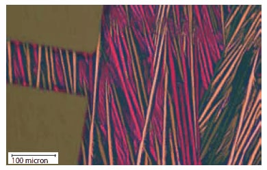
Figure 4.A device fabricated from TIPS pentacene 3c, showing highly oriented growth of the semiconductor.
Circuits
Despite the significant anisotropy in un-oriented films of TIPS pentacene, a number of complex circuits have been demonstrated using this material. The earliest approaches used vacuum-deposited films of TIPS pentacene (typical FET mobility: 0.002-0.05 cm2/Vs) onto pre-patterned Si/SiO2/Au substrates to yield an inverter with a gain of 5.5 at a driving voltage of -10 V.26 They also produced functioning NAND and NOR logic gates. More recent studies using solutiondeposited TIPS pentacene yielded average FET mobilities in the range of 0.2-0.6 cm2/Vs, and produced inverters with gain of 3.5.27 Sevenstage ring oscillators produced from these inverters yielded oscillation frequencies greater than 10 kHz, and operating voltages as low as -5 V.
Blends
To improve the film forming properties of small molecule semiconductors, the blending of molecule such as TIPS pentacene with insulating or semiconducting polymers has become a compelling strategy.28 The polymer matrix dramatically slows the loss of solvent from the spin-cast film, allowing the small-molecule to segregate and crystallize into large grains (Figure 5).

Figure 5.Micrograph of a polymer/TIPS pentacene blended film formed by dip-coating. Note the morphology of the TIPS pentacene crystals is similar to that seen in non-blended films (Figure 4).
This approach yields the processing properties of soluble polymer materials, with the excellent electronic properties of high-performance small molecules. Recent studies of poly(α-methylstyrene)/TIPS pentacene blends showed mobility as high as 0.54 cm2/Vs from spin-cast films.29 Detailed analysis of these films demonstrated that the semiconductor segregated preferentially to the interface with the silica dielectric, provided that a polymer of sufficiently high molecular weight was used. Blending TIPS pentacene with poly(triarylamine) semiconducting polymers led instead to segregation of TIPS pentacene to the top (air) interface of the polymer.30 In this case, spin-cast films in a top-gate configuration yielded saturation mobility as high as 1.1 cm2/Vs, with good device uniformity and stability.
Inkjet Printing
Inkjet printing is emerging as a leading technology for the deposition of organic semiconductor films in a variety of organic electronic applications.31 Early reports of printing of silylethyne-functionalized pentacenes demonstrated a need for careful selection of solvent blend, and relied on an unusual concentric ring arrangement of source and drain electrodes. With these precautions, average effective mobilities as high as 0.12 cm2/Vs were achieved when channel width was corrected to the actual portion of the channel region covered by crystallites.32 In late 2007, an all-inkjet-printed electrophoretic display was demonstrated using TIPS pentacene as the active transistor material.33 By exploiting short channel length devices, mobilities over 0.01 cm2/Vs could be achieved, allowing the fabrication of a backplane for the 10.5” 76 dpi display. We have achieved an average mobility of 0.194 cm2/Vs for all inkjet printed TFTs (channel length = 125 μm) made with TIPS pentacene in a polystyrene blended ink using bottom gate, bottom contact devices (Figure 6).
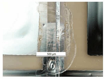
Figure 6.An inkjet printed transistor based on TIPS pentacene.
The electrodes and conductors were printed and sintered Ag nanoparticles, and the devices exhibited an on/off current ratio of 105, with an average threshold voltage and subthreshold slope of 0.148 V and 1.293 V/dec, respectively. An electrophoretic display driven by an all inkjet printed backplane is presented in Figure 7.
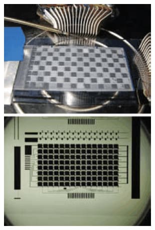
Figure 7.An all inkjet printed, TIPS pentacene based backplane (top) and an electrophoretic display made with that backplane (bottom).
Other Uses
TIPS pentacene has also found use as a donor in single-heterojunction solar cells (Figure 8). Solution deposited films of TIPS pentacene were paired with vacuum-deposited C60 (Product No. 572500) as an acceptor to yield solar cells with 0.52% efficiency.34 Alternatively, allvacuum- deposited single heterojunction cells with TIPS pentacene and C60 yielded solar cells with efficiency of 0.42%.35 Dioxole-functionalized derivative 5 performed somewhat better in these vacuum-deposited devices, yielding efficiencies up to 0.74%. Fullerene-based bulk heterojunction devices cannot be made with pentacene derivatives, due to rapid reaction between fullerenes and pentacenes.36 Derivative 5 is an intensely fluorescent compound, and has also been used to fabricate red organic light emitting diodes with external quantum efficiency of 3.3%.37
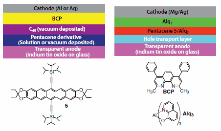
Figure 8.Top: Typical configurations for single-heterojunction organic solar cells (left) and light-emitting diodes (right). Bottom: dioxole derivative 5.
Conclusion
Soluble semiconductors are poised to play a leading role in emerging technologies. The structural variations exemplified by silylethynesubstitute pentacene have allowed tuning of the electronic, structural and film-forming properties of the important pentacene chromophore, yielding materials for both the study of intrinsic semiconductor properties in organic materials and exploration of the devices made possible by high-performance organic semiconductors. Combined with the straightforward synthetic routes to these materials, the avenues for exploration are nearly limitless.
Materials
References
To continue reading please sign in or create an account.
Don't Have An Account?