High Purity Metalorganic Precursors for Concentrator Photovoltaic Technologies Device Fabrication
Introduction to Solar Cells
Thin-film photovoltaic devices are important for efficiently harnessing solar energy to meet consumer demand. Conventional crystalline silicon solar cells have improved but still suffer from a range of natural limitations on efficiency, prompting the development materials that allow further advances. To date, the highest conversion efficiencies have been demonstrated using III-V compound semiconductors, and efforts are underway to integrate these materials into next generation architectures in a cost effective way. The high price of raw materials is a concern so thin film and concentrator photovoltaic technologies (CPV) are being targeted to reduce the quantity of the expensive semiconductor material required (for a given module size and power output).
To allow operation of miniature devices with reduced surface area and materials volume, highly advanced structures are required. The most attractive fabrication technique for III-V compound semiconductor layers is metal organic vapor phase epitaxy (MOVPE). The control of composition stoichiometries, layer thicknesses, and interface roughness achievable using MOVPE is key to minimize internal losses and increase overall conversion efficiencies. The demanding operating conditions (500 - 1,000 suns) place extreme stress on the device structure. Precise deposition of active layers, window/buffer layers and conducting oxide and/or metal electrode layers must be attained to maximize performance.
Selection and use of the appropriate chemical precursors is critical in the achievement of the highest quality layers using MOVPE. These materials must be of the highest purity and must be supplied to the deposition chamber in a uniform manner. This article discusses some of the issues related to the use of these precursors.
High Concentration CPV Multijunction Solar Cells
In a single band gap solar cell structure, such as those used in conventional crystalline silicon devices, one active layer is present to absorb photons. The conversion efficiency of the complete device is limited by the inability of this active material to absorb all of the photons impacting the device due to their broad range of energies. Photons with energies below the band gap of the active layer are lost because they are unable to provide sufficient energy to promote an electron to the required energy state and therefore pass through the layer unaffected. Photons with higher energies transfer only the energy required to perform the excitation and electron-hole pair generation for current extraction, with the remaining excess energy converted to heat. According to theoretical calculations, the maximum power conversion of a single band gap solar cell at standard conditions [AirMass (AM) 1.5] is about 30%.1 Conventional technologies are already reaching 23%, suggesting that further improvements will be increasingly difficult to achieve without a change in approach.
By using multiple junction solar cell designs with several different band gap materials, different portions of the solar spectrum may be converted at each junction, thus resulting in a cumulative effect leading to greater overall device efficiency. Figure 1 illustrates the combined use of three cells in a multijunction cell that match the incident spectral irradiation with the absorbing capabilities of the complete device structure.2 By modifying the individual layer compositions, improved matching of the absorption characteristics of the different sections can be achieved to increase the overall device photon capture capabilities. Beneficial changes can be made to the band gap engineering to customize cell properties for optimum performance in a particular region. These advances have led to a consistent improvement in device efficiencies.
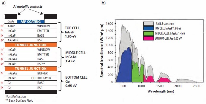
Figure 1.Multijunction solar cell (a) layer structure (b) spectral absorption.
The operation of the III-V multijunction device demonstrates improved performance when the impinging light is highly focused, hence mirrors and lenses are used to concentrate light onto the device up to 500 - 1,000 sun energy levels. These concentrator photovolatic (CPV) devices have been studied intensely, and the advances demonstrated in both materials performance and concentrator technologies have been significant (Figure 2).2 The current record efficiency for a three-junction, lattice-matched GaInP/GaInAs (1.4 eV)/Ge cell is 41.6%.3
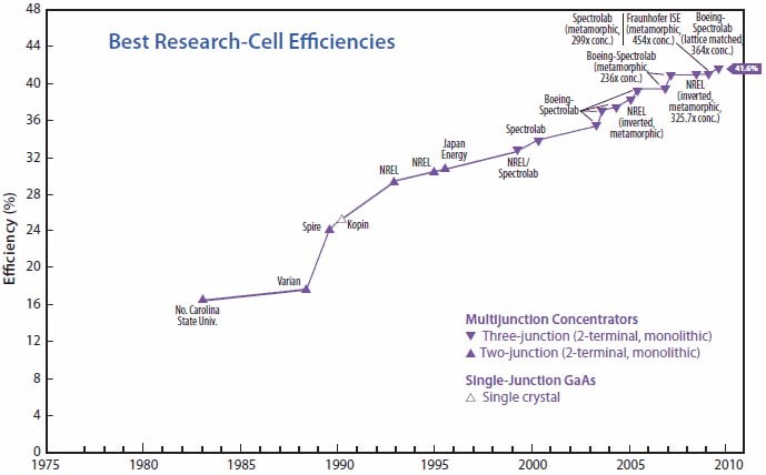
Figure 2.Historic summary of champion cell efficiencies for various photovoltaic technologies.2
Cell efficiencies have been increasing at a rate of about 0.5% to 1% per year and are expected to continue to increase toward 45% - 50% at the same pace. The implementation of additional cells in multijunction devices has been predicted to raise ideal values for 3-, 4-, and 5-junction cells to 47.3%, 49.3% and 50.5%, respectively.4 As concentrator technologies improve, the use of light falling on a larger area can be converted by the same size active multijunction cell as previously used. This scaling anomaly means that more electricity can be generated per unit volume of the expensive semiconductor to reduce cost. Coupled with the high conversion efficiency at high illumination concentrations to further increase output, CPV is clearly promising as the next power generation technology.
MOVPE Process
The basic MOVPE process was first demonstrated in the 1970s for GaAs thin film formation. Since then, the fundamentals have not changed, although the complexity of layer compositions and combinations has increased dramatically. MOVPE differs from the more generic metal organic chemical vapor deposition (MOCVD) technique only in the nature of the films deposited. MOCVD encompasses amorphous, polycrystalline and epitaxial films, while MOVPE focuses solely on the epitaxial films. The technique involves passing vapors containing the individual components required for the target film into a deposition chamber containing a heated substrate. The vapors flow over the substrate and are thermally decomposed to deposit a coating, with the by-products swept away from the surface by the carrier gas (Figure 3). By changing the precursor-supply ratios, films with different stoichiometries can be deposited. The control of this process is the key factor in the production of advanced devices.
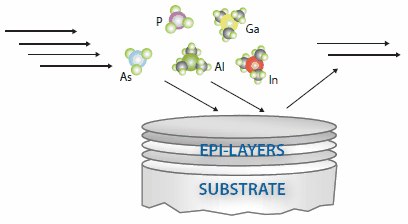
Figure 3. Illustration of MOVPE process.
The generation of precursor vapors is achieved by passing a carrier gas through the liquid or solid chemical reservoir. Saturating the gas stream is desired so that the precise uptake of precursor into the gas phase is constant per unit volume, even when changing flow rates. A known amount of chemical is then delivered to the deposition chamber by controlling the volume of this saturated gas. To achieve constant saturation levels, the design of the precursor container has been modified, as described later in this article.
MOVPE of compound semiconductors use highly reactive, toxic and pyrophoric precursors, which present numerous challenges to handling, purification and use. The main products used for Group III metal sources are trimethyl derivatives; namely trimethylgallium (Me3Ga, TMGa), trimethylaluminum (Me3Al, TMA) and trimethylindium (Me3In, TMIn). The Group V sources used are hydrides; namely arsine (AsH3) and phosphine (PH3). The thorough mixing of precursor vapors in the chamber and minimization of interactions between them to form particles, has been optimized so that highly uniform films can be deposited.
In today′s process tools, multiple substrates are coated in each deposition run. Complex holders are used that rotate during the run to increase the uniformity of the deposited layer over the whole of the substrate area. This motion also improves reproducibility between wafers and batches. These advanced technologies enable the fabrication of large numbers of devices for inclusion into solar cell modules for increased installed power generation. In comparison with molecular beam epitaxy (MBE), which can also produce some of the complex III-V structures needed, MOVPE is more cost effective.
III-V Compound Semiconductor
The structure of the complete cell must be as perfect as possible, as the active components are under highly demanding conditions. Similarly, to avoid unwanted internal losses due to non-radiative centers and the generation of excessive heat, the number of metallic contaminants must be exceptionally low. This stipulation demands ultra-high precursor purities to avoid contaminant introduction with the vapors passed into the reaction chamber. Proprietary processes must be used to isolate final chemicals with sub-ppm impurity concentrations and strict handling protocols must be used to avoid contamination prior to introduction to the substrate. Significant experience in the area of III-V semiconductor high brightness LED production can be accessed to provide chemicals of the targeted quality in a manner suited to high volume usage with the degree of control required to afford the highest device performance.
In particular, it has been observed that oxygen (O) is an unwanted non-radiative center that detracts from cell operating efficiencies and lifetimes. To minimize O levels in the deposited films, the precursors used must be of the highest quality and, in particular, the organoaluminum source must have contaminant levels less than 1 ppm. Figure 4 shows the detected O species levels in a series of Me3Al samples and Table 1 highlights the properties of aluminum gallium arsenide (AlGaAs) deposited using these samples. A direct correlation between the two sets of data is clearly seen, with contamination levels of less than 1 ppm in the source shown to be the key to achieving the highest final film quality.5
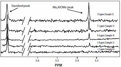
Figure 4.Proton NMR determination of -OMe content in different Me3Al samples.
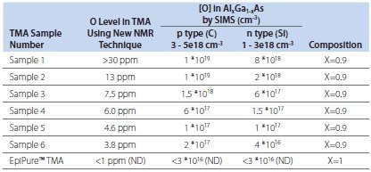
Table 1.Secondary Ion Mass Spectroscopy (SIMS) data for O impurity levels in MOVPE deposited AlGaAs films.
At these ultra-low contamination levels, the equipment used to perform the MOVPE growth must also be of the highest quality. Leak testing and surface pretreatments must be rigorously applied to ensure other O sources are minimized. For the trials performed, the batch to batch reproducibility of the state of the growth system used was checked with repeat runs and a number of standard correlations to ensure the only variable was the Al precursor.
In a similar manner, direct correlation between metallic impurity levels, carrier numbers and carrier mobilities can be made, illustrating the need for complete removal of contaminants from sources used in MOVPE.
Precursor Vapor Transport
The delivery of a constant precursor gas-phase concentration is critical to the development of MOVPE processes. To achieve the levels of control necessary for the high quality films targeted, the supply must be stable over a wide range of operating conditions. In particular, interface abruptness is needed to avoid charge trapping and device degradation, and is highly dependant on precursor delivery control. To optimize the absorber efficiency, strict stoichiometric control of the alloy composition is critical and thus the vapor phase concentration of the precursors entering the growth chamber must be precisely metered, not only during one growth but over the lifetime of the chemical source. The vessel design has been studied intensively with a variety of approaches proposed to achieve the degree of reproducibility demanded. Initially, simple containers with a single diptube (bubblers) were used, but as their volumes increased, the efficiency of vapor saturation was found to decrease toward the end of a batch. This drop off led to premature change out and lost production time. For liquids, a convenient solution for larger bubblers (>75 mm diameter) is the use of a cross dispersion arrangement at the end of the diptube. (Figure 5a) This device effectively spreads the carrier gas through the liquid, leading to complete vapor saturation over an extended fill level range, increasing the useable time for the source and reducing residual chemical at end of life.
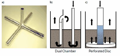
Figure 5.Improved pick up efficiency approaches (a) Cross dipleg and (b) dual chamber (c) disc vessel.
The above methodology is not effective for solid precursors and more complex container geometries must be applied. The main objective of the container design is to increase the contact time between the carrier gas and the precursor to allow the most efficient vaporization possible. While it is relatively easy to achieve efficient vaporization with a full vessel, as the precursor is depleted, non-uniformities occur to form channels in the solid precursor where material has been removed. Gas passing through these channels has a reduced contact time with the precursor, leading to a drop in the vapor concentration achieved under identical flow conditions with a full vessel. To minimize the variance in precursor removal across the vessel cross section, several designs have been effectively demonstrated, including frit and perforated disc supports.6, 7 These supports ensure a laminar flow of gas passes through the solid. In combination with the use of multiple chambers, this provides much improved performance (Figures 5b and 5c). As batch volumes increase further, the requirement for innovative new vessels will again need attention to maximize the output stability of precursor vapors over the extended source lifetimes. This area remains one of the most challenging topics for industry scale-up and must be solved to allow true large area deposition of multijunction III-V devices required for commercialization.
Computer modeling is now being used to develop improved vessels, and typical data are shown in Figure 6 where gas flows are calculated (6a) and output fluxes generated (6b) for the most studied solid precursor, Me3In (TMIn). It should be noted that the predicted stability and usage is a significant improvement on the state of the art, and initial testing of a prototype vessel has achieved these levels of output stability over an extended range of trial conditions.
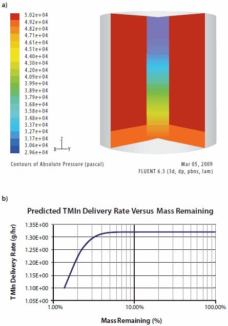
Figure 6.(a) Modelling of gas flows (b) output flux calculations for advanced vessel designs.
High-efficiency CPV Device Example
Use of high purity metal organic precursors in a controlled fashion to fabricate precise layer structures has been an enabling technology for improved performance CPV devices. A recent example of a device from Fraunhofer ISE8 with over 40% efficiency is illustrated in Figure 7. A three PN-junction combination of gallium indium phosphide (Ga0.35In0.65P), gallium indium arsenide (Ga0.83In0.17As) and germanium (Ge) is used. Absorption of sunlight in the ranges 300 - 780 nm, up to 1,020 nm and up to 1,880 nm is achieved by the different materials (Figure 1b), which has been predicted as particularly advantageous for optimizing conversion of the terrestrial solar spectrum to electricity.
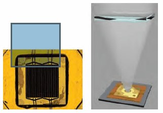
Figure 7.Fraunhofer ISE high efficiency multijunction solar cell (a) active component (b) whole device.8
The solar cell has a cell area of 5.09 mm2 and a 41.1% overall efficiency when operated at 454 suns. The ability to operate at even higher concentrations while maintaining high efficiency (37.6% @ C = 1,700) is a key advantage of this cell design, but this function is significantly dependant on perfect construction of all the individual layers and interfaces to avoid charge trapping and the more problematic defect propagation. The degradation of quality by such effects leads to reduced lifetimes, which are not acceptable in a commercial device. Hence, the focus on deposition technologies is to achieve high quality epitaxy throughout the multilayer structure. Similarly the impurity levels must be extremely low to avoid loses through heat generation. The ability to achieve close to theoretical outputs indicates that the materials used were of the correct quality to ensure minimal contributions from this loss mechanism.
Summary
For the delivery of highly concentrated sunlight onto a small-area, highly efficient (~40%) converter has the potential to provide a cost-effective approach to solar-electricity generation (especially in sunny locations). Fabrication of advanced thin-film multijunction solar cells is moving toward large-scale manufacture, and this industry is ready for substantial growth in the next years as the world enthusiastically embraces solar energy. MOVPE will be the technology of choice for production of these specialized cells, and the metal organic precursors used need to be of the highest purity to maximize performance and enable robust, cost-effective processes to be implemented to meet demand in this exciting field.
Materials
To continue reading please sign in or create an account.
Don't Have An Account?