Nanocomposite Coatings with Tunable Properties Prepared by Atomic Layer Deposition
Introduction
Nanocomposite coatings, comprised of a precisely blended mixture of components, have diverse applications in microelectronics, optics, sensors, and solid-state detectors. By varying the composition of the mixture, the electrical, optical, and physical properties of the coatings can be “tuned” over almost the full range of the individual components, and can sometimes yield properties distinct from those of any of the constituents. There are many techniques for producing nanocomposite coatings, but atomic layer deposition (ALD) is particularly well suited for controlling the properties of the fabricated coatings. ALD uses alternating cycles of gaseous precursors to a solid surface to deposit materials in an atomic layer-by-layer fashion.1 Because a chemical reaction on the surface naturally terminates when the surface functional groups are all reacted, the amount of material deposited in one ALD cycle is easily controlled. This self-limiting property, coupled with facile diffusion of the precursor vapors into narrow pores and voids, allows complex, 3-dimensional substrates to be coated with excellent uniformity and conformality.2 ALD can be used to deposit a wide variety of materials including metal oxides, nitrides, sulfides, and even pure elements. By alternating between two materials (e.g., a metal and a metal oxide), we can synthesize complex nanocomposite coatings.3–5 The thickness of the coating is controlled by the total number of ALD cycles performed, and the composition is controlled by the ratio of the ALD cycles executed for each of the two components.
In this study, we employed in situ quartz crystal microbalance (QCM) measurements and Fourier transform infrared (FTIR) absorption spectroscopy to investigate the ALD growth mechanism of nanocomposite films comprised of Mo:Al2O3 and W:Al2O3. These films were prepared using alternating exposures to trimethyl aluminum (TMA) and H2O for the Al2O3 ALD, and alternating MF6/Si2H6 exposures for the metal ALD, where M=Mo or W. In the case of the Mo:Al2O3 films, QCM showed that the Mo ALD inhibits the Al2O3 ALD and vice versa. Despite this inhibition, the relationship between Mo content and Mo cycle percentage was easily controlled. Surprisingly, FTIR revealed that the reducing agent for the Mo was not the Si2H6, but rather the TMA exposure from the subsequent Al2O3 ALD cycle. Elemental analysis showed that the M:Al2O3 films were uniform in composition and contained Al, O, and metallic Mo or W as expected, but also included significant F and C. Cross-sectional transmission electron microscopy revealed the film structure to be metallic nanoparticles (~1 nm) embedded in an amorphous matrix.
Three distinct practical applications of this technology are explored in this paper. We utilized these nanocomposite coatings to functionalize capillary glass array plates to fabricate largearea microchannel plates (MCPs) suitable for application in large-area photodetectors. In addition, we applied these films as charge drain coatings in electron-optical microsystems for a prototype electron beam lithography tool, permitting highresolution electron beam patterns without charging artifacts. Finally, we explored the suitability of these films for use as selective solar absorbing coatings in concentrated solar power.
Experimental
Deposition of the Mo:Al2O3 and W:Al2O3 composite ALD film was performed at 200 °C in a hot-walled viscous flow ALD reactor.6 This reactor was equipped with a quartz crystal microbalance (QCM) that allowed In situ studies of the ALD processes. The TMA (97%, Sigma-Aldrich), deionized H2O, Si2H6 (99.998%, Sigma-Aldrich), MoF6 (99%, Alfa Aesar), and WF6 (99.8%, Sigma- Aldrich) precursors were maintained at room temperature. The ultrahigh purity (99.999%) N2 carrier gas flow was set to 300 sccm, which provided a base pressure of 1.0 Torr in the ALD reaction chamber as measured by a heated Baratron pressure gauge (MKS model 629B). The Mo:Al2O3 and W:Al2O3 composite films were deposited on n-type Si(100) substrates. Prior to ALD, the substrates were cleaned using a 10 min ultrasonic treatment in acetone. For the Al2O3 ALD, TMA and H2O were alternately pulsed into the N2 carrier flow with the following sequence: 1s TMA dose (0.2 Torr) – 5s purge – 1s H2O dose (0.3 Torr) – 5s purge. Similarly, the Mo and W ALD used alternating exposures to MoF6/Si2H6 and WF6/Si2H6, respectively, with the timing sequence: 1s Si2H6 dose (0.25 Torr) – 5s purge – 1s MoF6 or WF6 dose (0.05 Torr) – 5s purge. These conditions for the Al2O3, Mo, and W ALD provided self-limiting growth as verified by In situ QCM measurements.
In situ QCM was performed to examine the Mo:Al2O3 and W:Al2O3 composite ALD using different ALD pulse sequences. The QCM measurements typically used 10s N2 purge times to allow the QCM signal to stabilize after each precursor exposure. Transmission electron microscopy (TEM) analysis was performed by Evans Analytical Group (Sunnyvale, CA). TEM samples were prepared using the In situ focussed ion beam (FIB) lift out technique on an FEI Strata Dual Beam FIB/SEM. The samples were capped with a protective layer of carbon prior to FIB milling, and were imaged with a FEI Tecnai TF-20 FEG/TEM operated at 200 kV in bright-field (BF) TEM mode, high-resolution (HR) TEM mode, and nanobeam diffraction (NBD) mode. The composition of the Mo:Al2O3 and W:Al2O3 composite layers was determined by depth profiling using X-ray photoelectron spectroscopy (XPS, Evans Analytical Group) and Rutherford backscattering spectroscopy (RBS, Evans Analytical Group). The metal content in the composite films was measured using X-ray fluorescence (XRF, Oxford ED2000).
The resistance of the Mo:Al2O3 and W:Al2O3 composite layers was determined by performing current-voltage (I-V) measurements using a Keithley Model 6487 current-voltage source. To facilitate I-V measurements on these highly resistive coatings, the films were deposited on insulating substrates with lithographically patterned comb structures comprised of interdigitated Au electrodes with a 2 μm spacing.7 These comb structures provided an 80,000 times greater effective contact area, and an equivalent boost in current compared to conventional four-point probe measurements. Additional I-V and electron amplification measurements were performed on W:Al2O3 layers deposited on high aspect ratio (60:1) borosilicate glass capillary arrays with 20 μm pores fabricated by Incom, Inc. (Charlton, MA). These capillary arrays were also coated with an eight nm ALD MgO emissive layer to boost the secondary electron coefficient, and both sides were coated with 100 nm evaporated nickel-chromium to provide a low resistance electrical contact.
In situ Fourier transform infrared (FTIR) measurements were performed during the Mo:Al2O3 ALD using a Nicolet 6700 with a liquid nitrogen-cooled MCT-B detector. For these measurements, the FTIR beam was diverted through CsI windows and into the ALD reactor. The windows were protected by gate valves, which were closed during the ALD exposures to prevent deposition on the windows. The FTIR beam was directed through a sample comprised of ZrO2 nanopowder pressed into a stainless steel grid to enhance the sample surface area and boost the optical absorption.8 Prior to the Mo:Al2O3 ALD, the ZrO2 powder was coated using 10 cycles of TMA and H2O for Al2O3 ALD.
Results and Discussion
Growth and Properties of Mo:Al2O3 Composite Films
Figure 1 shows a schematic of the precursor dosing strategy used to synthesize the Mo:Al2O3 ALD composite films. Alternating TMA/H2O exposures were used to deposit Al2O3, and periodically a single MoF6/Si2H6 cycle was performed to introduce the Mo. We define the Mo cycle percentage as: %Mo=Mo/(Mo+Al2O3)*100 where Mo and Al2O3 are the relative numbers of TMA/H2O and MoF6/Si2H6 cycles performed, respectively. Because of the drastically different resistivity for these two materials (~1016 and 10–4 Ohm cm for Al2O3 and Mo, respectively), we expected to be able to tune the resistivity for the composite film over a broad range by adjusting the Mo cycle percentage.

Figure 1. Schematic illustration of precursor pulsing sequence for ALD of Mo:Al2O3 nanocomposite coating using alternating TMA/H2O exposures for the Al2O3 ALD and alternating MoF6/Si2H6 exposures for the Mo ALD.
Figure 2A shows in situ QCM measurements performed during the ALD of a Mo:Al2O3 composite film using a 10% Mo cycle percentage (nine Al2O3 ALD cycles followed by one Mo ALD cycle). The overall pattern consists of nine small mass gains followed by a single, larger mass gain, and this pattern is repeated three times. Figure 2B shows an expanded view of the boxed region in Figure. 2A and reveals some informative details about the QCM mass gains. Between 95–115s, two TMA/ H2O cycles for Al2O3 ALD are shown and the QCM signals match the expected pattern for Al2O3 ALD.3 The net mass gain for each Al2O3 ALD cycle is ~30 ng/cm2, which is slightly smaller than the expected value. In contrast, the QCM signals observed during the MoF6/Si2H6 exposures do not follow the pattern reported in the literature for Mo ALD.9 In particular, no mass gain is observed during the Si2H6 exposure, and the net mass gain is only ~250 ng/cm2, which is far below the 1,000 ng/cm2 expected for Mo ALD. It is interesting to note that the first TMA exposure following the Mo ALD cycle yields a sharp mass rise followed by a slow decay. This is the signature pattern for a temperatureinduced QCM transient produced by an exothermic reaction.10
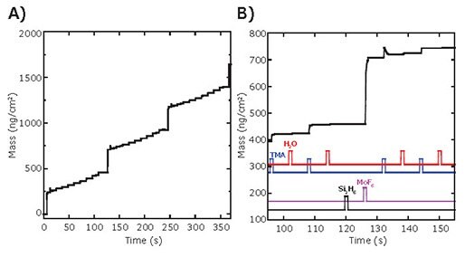
Figure 2. In situ QCM measurements during Mo:Al2O3 composite film ALD using a 10% Mo cycle percentage (nine Al2O3 ALD cycles followed by one Mo ALD cycle). A) Mass vs. time over 30 ALD cycles. B) Expanded view of the inset in A, with TMA, H2O, Si2H6, and MoF6 dose times are indicated.
Figure 3 shows the net mass gains following each ALD cycle for Mo (triangles) and Al2O3 (circles). The dashed, horizontal line shows the expected, steady-state mass gains for Al2O3 ALD at ~35 ng/cm2. This figure illustrates that the Al2O3 ALD is inhibited by ~50% initially following the Mo ALD, and does not quite achieve the steady-state value even after nine Al2O3 ALD cycles. Moreover, the Mo ALD is also severely inhibited on the Al2O3 surface by ~75%.
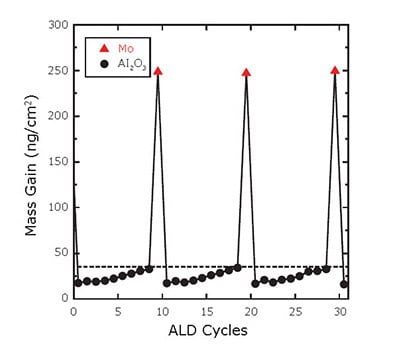
Figure 3. Net mass gains following each ALD cycle of Mo:Al2O3 composite film deposition using a 10% Mo cycle percentage. Mo and Al2O3 ALD cycles are indicated by the triangles and circles, respectively. The dashed, horizontal line shows the expected steady-state mass gain of 35 ng/cm2 for Al2O3 ALD.
The origin for some of the unusual QCM results can be gleaned from the in situ FTIR measurements. Figure 4 shows the IR absorbance at 4000 cm-1, measured following the individual precursor exposures, where the precursor pulsed immediately prior to recording the IR spectrum is indicated above each data point. The 4000 cm-1 frequency was selected because it falls in a spectral region where there are no peaks from any of the surface functional groups, and therefore serves as an indirect measure of the relative conductivity of the film.11 The IR absorbance at 4000 cm-1 remains relatively constant during the TMA and H2O exposures for Al2O3 ALD. We might expect the IR absorbance to increase during the Si2H6 exposures for the Mo ALD since Si2H6 is believed to be the reducing agent for the Mo.9 However, this is clearly not the case, as there is practically no change in the IR absorbance during the Si2H6 exposures. Instead, the IR absorbance increases sharply during the TMA exposures that follow the MoF6 exposures. This finding suggests that TMA is in fact the reducing agent, which is consistent with the exothermic transients seen in the QCM data during the TMA exposures following MoF6 exposures (Figure 2B). Additional evidence for the reducing effect of TMA on the adsorbed MoF6 was indicated by a decrease in the MoOFx stretching frequency at 1040 cm-1 during the TMA exposures (spectra not shown).

Figure 4. IR absorbance at 4000 cm-1 measured by in situ FTIR following individual precursor exposures for the Mo:Al2O3 composite film ALD. The precursor pulsed immediately prior to recording the IR spectrum is indicated above each data point.
Figure 5 shows a low-resolution cross-sectional TEM image of a 40 nm Mo:Al2O3 composite film prepared on a Si(100) substrate using 10% Mo cycles. This film appears dense and continuous, and the top surface is relatively smooth and parallel to the Si substrate. The interface between the Si substrate and the Mo:Al2O3 composite film shows a low density, amorphous region attributed to the Si native oxide and Al2O3 from the initial ALD cycles. Under higher resolution (Figure 5A), the Mo:Al2O3 composite film is seen to consist of 1–2 nm particles (dark spots) embedded in a lower density matrix. Close inspection of the particles (Figure 5A, inset) reveals weak lattice fringes. Moreover, nano-beam diffraction measurements acquired from the nanocomposite film (Figure 5B) exhibit diffuse rings consistent with crystalline nanoparticles. Based on these observations, and on our previous study of the W:Al2O3 composite film ALD,5 we hypothesize that the crystalline nanoparticles in Figure 5A are metallic Mo. These Mo nanoparticles might form through the sintering of Mo atoms upon reduction of MoOFx surface species by the TMA. The role of TMA as a reducing agent is somewhat surprising, but we believe this to be true based on our FTIR results, and because the microstructure and properties of the Mo:Al2O3 composite films are practically identical when the Si2H6 exposures are not performed.
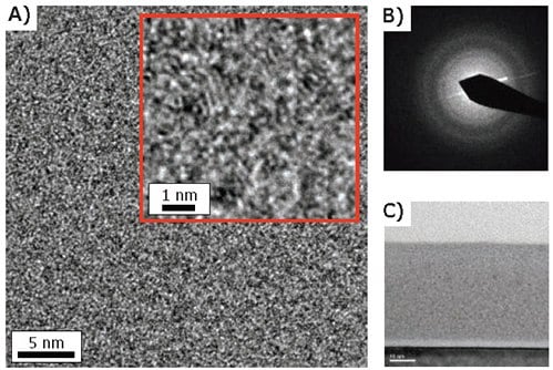
Figure 5. Cross-sectional TEM analysis of 40 nm Mo:Al2O3 composite film prepared on Si(100) substrate using 10% Mo cycles. A) High resolution image showing 1–2 nm particles (dark spots) embedded in a lower density matrix. B) Nano-beam diffraction of film region shown in A. C) Low resolution image of entire film thickness.
The composition of the Mo:Al2O3 composite films was determined using XPS depth profiling and RBS measurements of films prepared on Si(100) substrates. These measurements revealed that the films contained Al, O, and Mo as expected, but also contained ~5% C and ~10% F. XPS demonstrated that Mo exists in both the metallic and sub-oxide (Mo+4) states in the film. These findings, when combined with the QCM and FTIR measurements, suggest that the TMA reduces the adsorbed MoOFx species to form AlF3 and metallic Mo. In addition, the C and F presence in the films is similar to that in a previous study which concluded that alternating exposures to NbF6 and TMA produced films comprised of NbFx, NbC, C, and AlF3.12
Next, a series of Mo:Al2O3 composite films was prepared on Si(100) substrates using different Mo cycle percentages and analyzed by X-ray fluorescence to determine the Mo content of the films. As shown in Figure 6A, the Mo content increases linearly from 2.1 to 9.0 mol% Mo as the Mo cycle percentage increases from eight to 15% Mo. This linear relationship demonstrates that the Mo content can be easily and precisely controlled by adjusting the Mo cycle percentage during the Mo:Al2O3 composite film ALD. The resistivity of the Mo:Al2O3 composite films was determined using current-voltage measurements of films deposited on comb structures, and the results are shown in Figure 6B. Figure 6B shows that the resistivity of the Mo:Al2O3 composite films can be tuned over a very broad range by adjusting the Mo cycle percentage. The range of resistivity values provided by these coatings (104–1010 Ohm cm) is particularly useful for applications in electron multipliers and charge drain coatings, and this capability will be demonstrated below.
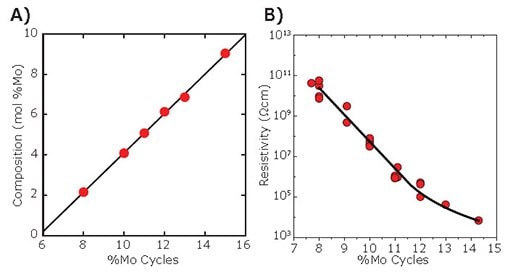
Figure 6. A) Mo content of ALD Mo:Al2O3 composite films as determined by XRF measurements versus Mo cycle percentage. B) Resistivity of ALD Mo:Al2O3 composite films as determined by current-voltage measurements versus Mo cycle percentage.
Growth and Properties of W:Al2O3 Composite Films
We performed in situ QCM measurements of the W:Al2O3 composite film grown by ALD to explore their growth behavior. We deposited and characterized a range of W:Al2O3 composite films while varying the W cycle percentage to determine the thickness, composition, morphology, and microstructure of these films and to establish the effect of W content on resistivity.5 Some of these results are presented in Figure 7.
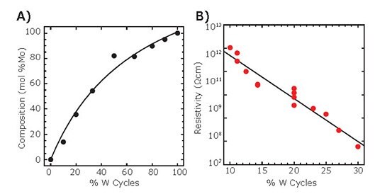
Figure 7. A) W content of ALD W:Al2O3 composite films deduced from in situ QCM versus W cycle percentage. B) Resistivity of ALD W:Al2O3 composite films determined by current-voltage measurements versus W cycle percentage.
Figure 7A shows the composition of the W:Al2O3 composite films as determined by in situ QCM versus W cycle percentage. The W mol% varies smoothly over the full range, and is approximately linear between 10–30%. Figure 7B shows the effect of varying the W cycle percentage on the resistivity as determined by current-voltage measurements of films deposited on comb chips and on capillary glass array substrates. The resistivity decreases approximately exponentially from ~1012 Ohm cm at 10%W cycles to ~108 Ohm cm at 30% W cycles. This behavior is similar to that of the Mo:Al2O3 composite films (Figure 6B), although the slope is much steeper in the case of the Mo:Al2O3 composite films (6 decades over 4% change in Mo cycles) as compared to W:Al2O3 composite films (4 decades over 20% change in W cycles). This difference may stem from the much higher deposition rate for the Mo (~10 Å/cycle)9 versus the W (~4 Å/cycle)13 under similar growth conditions, especially in light of the exponential relationship between resistivity and metal content.
Next, we performed optical absorption measurements on the W:Al2O3 composite films prepared using 0–60% W cycles. The direct bandgaps were extracted from the absorption spectra using Tauc plots, and the results are shown in Figure 8A. The bandgap decreases with increasing W cycle percentage. Figure 8B shows the absorption coefficients as a function of photon energy for these coatings and clearly shows that the absorption onset shifts to lower energies with increasing W cycle percentages between 10–40%, and then transitions to a broadband, metallic absorption for the higher W cycle percentages of 50–60%. This tunable absorption property is desirable for selective solar absorption coatings that must absorb visible light while transmitting or reflecting infrared wavelengths, as discussed next.

Figure 8. A) Direct bandgap versus W cycle percentage and B) absorption coefficient versus photon energy for ALD W:Al2O3 composite films prepared using 0–60% W cycle percentage.
Other Nanocomposite Coatings
Similar to the coating strategies previously described, we have developed ALD methods for nanocomposite coatings using combinations of W, Mo, Ta, Nb, and Co metals, and Al2O3, ZrO2, HfO2, MgO, and TiO2 dielectrics. Although a complete description is beyond the scope of this article, we note that the trends of increasing electrical conductivity, decreasing bandgap, and increasing absorption coefficient with increasing metal content are common to all of these materials.
Applications for Tunable Resistance Coatings
Microchannel Plates (MCPs)
Microchannel plates (MCPs) are solid-state electron amplifiers comprised of a two-dimensional array of microscopic channels in the form of a thin, flat plate. MCPs are used in detectors to identify low levels of electrons, ions, photons, or neutrons, and provide an amplified response via gain from secondary electron emission that occurs within the individual channels of the MCP.14 This unique quality allows MCPs to form images, and is critical to a wide variety of detectors and devices. Conventional MCP fabrication involves using multi-fiber glass working techniques to draw and assemble an array of solid-core fibers into a block. The block is subsequently sliced into thin wafers, and the solid cores are chemically etched to form an ordered array of pores comprised of lead silicate glass. Hydrogen firing is then used to activate the channel walls for electron multiplication. One drawback of this process is that the electrical conductivity and the secondary electron emission properties of the MCP cannot be adjusted independently, because both of these properties are imparted during the hydrogen-firing step. An additional drawback is that the aspect ratio (pore length to pore diameter) of the pores is limited to ~100 because the chemical etchant cannot diffuse into longer pores without dissolving the lead silicate cladding. This limits the gain that can be achieved.
An alternative strategy for MCP manufacturing is to functionalize glass capillary array wafers using ALD to impart the necessary conductivity and secondary emission properties.15,16 This process is illustrated in Figure 9 for a 1.2 mm thick, 33 mm diameter disc with a pore size of 20 μm (Figure 9A-C). Figure 9D shows the 33 mm capillary array disc after ALD of a 94 nm Mo:Al2O3 composite film to serve as a resistive layer, and an 8 nm ALD MgO to enhance the secondary electron emission of the surface.17 After the ALD, nickel-chromium electrodes were evaporated onto both sides of the disc to generate the MCP shown in Figure 9E. The ability to tune the resistivity of the ALD composite film allows MCPs to be manufactured over a broad resistance range so as to be optimized for specific detector applications.
The fully functionalized MCP shown in Figure 9E was evaluated in a high vacuum system equipped with a calibrated electron source and a phosphor screen to determine its gain and spatial uniformity. As shown by the photograph of the phosphor screen image in Figure 9F, the MCP response is uniform across the surface. Next, a pair of identical MCPs was assembled in series and installed in front of a position-sensitive anode. Using a photon counting mode and weak ultraviolet illumination, a two-dimensional map of the spatial distribution of the gain was generated (Figure 9G), again showing the uniformity of the gain across the MCP. Studies on the performance of ALD MPCs have also been reported.14
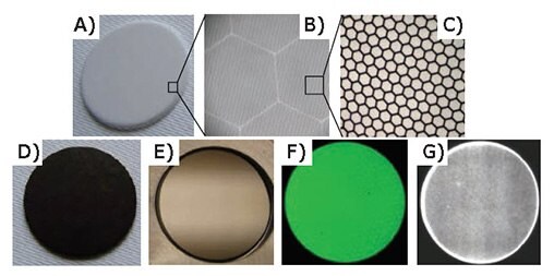
Figure 9. MCP fabrication using ALD tunable resistance coatings. A-C) Increasing resolution of 33 mm diameter borosilicate glass capillary array substrate comprised of hexagonal bundles of 20 μm pores. D) Glass substrate after 94 nm ALD Mo:Al2O3 composite resistive layer and eight nm ALD MgO emissive layer. E) Completed MCP with nickel-chromium electrodes. F) Phosphor screen illuminated with electrons amplified by ALD MCP. G) Gain map for pair of ALD MCPs.
One of the benefits of using ALD for MCP manufacturing is that it facilitates scaling to larger detector sizes. The dark circular disk in Figure 10 is the 33 mm MCP described above. To the left of this small MCP is an 8 x 8” glass capillary array substrate in a metal transport case. To the right is an identical 8 x 8” plate after ALD functionalization and electrode deposition to produce a large-area MCP. This is the largest MCP ever produced. Work is underway in the Large Area Picosecond Photodetector Project led by Argonne National Laboratory to implement these MCPs for applications in high-energy physics.14,15
Charge Drain Coatings Electrostatic charging is a challenging problem in electronoptical devices such as mass spectrometers, particle detectors, and micro-electro mechanical systems (MEMS). When stray electrons strike the surfaces of insulating components in a vacuum environment, the electrons become trapped, creating an electrostatic charge. With no means of draining the accumulated electrostatic charge, which can generate potentials of several kilovolts, the local electric fields become distorted causing loss of focus, resolution, and timing. Simple conducting or semiconducting films are unsuitable for draining this charge because the high leakage current can exceed the power supply or damage the device through resistive heating. Instead, a thin film with resistivity in the mesoscale (between those of a semiconductor and an insulator, 102–107 Ohm cm), is needed. In electron-optical MEMS, the challenge is aggravated by the much closer proximity of the electrons to the surfaces, and the films are subjected to very high electrical fields of up to 25 MV/m. Furthermore, the film must coat all surface orientations while maintaining nanoscale uniformity to ensure equivalent performance across all components.

Figure 10. Uncoated 8 x 8” glass capillary substrate in metal transport case (left) next to identical, 8 x 8” glass substrate after ALD Mo:Al2O3 composite coating. Ruler and 33 mm MCP are shown for scale.
The ALD tunable resistance nanocomposite films are an excellent candidate for charge drain coatings. We have demonstrated their benefit in the reflective electron beam lithography (REBL) Nanowriter — a high throughput, direct-writing, maskless lithography tool under development at KLA—Tencor.18 A schematic of the Nanowriter is shown in Figure 11A. The heart of the patterning system is the digital pattern generator (DPG) chip (Figure 11B). The DPG is an integrated circuit chip with an array of small, independently controllable electron mirrors (“lenslets”) producing over 1 million “beamlets”. The lenslet electrode MEMS structure is fabricated on top of complementary metal oxide semiconductor (CMOS) circuitry that provides voltage to four electrodes per lenslet to establish the electric fields required to produce an electrostatic lens for each pixel. The pixels and lenslets of the array are located on a 1.6 μm pitch, and the lenslet structure is ~four μm in height. The DPG chip operates under a constant illumination of electrons, and this can lead to electrostatic charging on the insulating oxide surface along the wall of the lenslet (Figure 11C) that reduces the image quality (Figure 12G). To overcome this problem, a KLA-Tencor DPG chip was coated using an ALD Mo:Al2O3 composite coating to drain static charge (Figure 11D). Figures 12A–F show images of electron beam test patterns obtained using this DPG. These images indicate virtually defect-free DPG patterns.19

Figure 11. A) Schematic of KLA-Tencor REBL Nanowriter. B) REBL digital pattern generator (DPG). C) Cleaved cross-section of DPG MEMS lenslet array structure. D) Schematic of ALD charge drain coating covering DPG lenslet array.

Figure 12. Defect-free test pattern images from DPG coated using ALD Mo:Al2O3 composite charge drain coating. A) Square pattern, B) chevron pattern, C) stitching pattern, D) stig test pattern, E) KLA-Tencor company logo, and F) contact hole pattern. G) Poor quality pattern from DPG without ALD Mo:Al2O3 charge drain coating.
Solar Selective Coatings
Concentrated solar thermal power combines both energy harvesting and energy storage in a single plant, making it very appealing. Solar “power tower” facilities can generate hundreds of megawatts using a vast array of mirrors to reflect solar radiation onto a central receiver, where the energy is absorbed and used to heat a fluid that can be stored, or used to drive a turbine for electric power (Figure 13A). The efficiency can be increased using a solar-selective coating that absorbs strongly in the visible solar spectrum, while simultaneously reflecting infrared (IR) wavelengths. A high IR reflectivity ensures that the receiver will not radiate IR energy at high operating temperatures, allowing more of the energy to be captured and used. In addition, the coating must endure high temperatures without losing its selective absorption properties. As described above, the optical absorption of the ALD W:Al2O3 composite films can be tuned by adjusting the W content. This coating can be deposited on a metal substrate to absorb visible light while reflecting IR wavelengths. We prepared a 100 nm ALD W:Al2O3 composite film using 33% W cycle percentage on a Hayes 230 nickel superalloy coupon that had been pre-coated with a high surface area mesoporous film. The resulting material is opaque in the visible, but highly reflective in the IR. Figure 13B shows the substrate after 12 hours in air at 800 °C, and 50 thermal shock cycles between 300–800 °C in air. Most conventional materials would oxidize during this treatment and become transparent, but our ALD nanocomposite coating is extremely stable at high temperatures in air, and remains black. Moreover, our coating resists cracking and delamination during repeated thermal cycling that simulates the day-night temperature changes. These ALD materials are very promising for use as selective solar absorbing coatings in next-generation concentrated solar thermal power facilities.
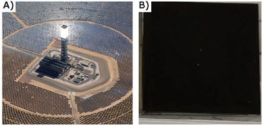
Figure 13. A) Aerial photograph of Ivanpah concentrated solar thermal power facility showing array of mirrors focussing sunlight on central receiving tower. B) 100nm ALD W:Al2O3 composite films prepared using 33% W cycle percentage on Hayes 230 nickel superalloy coupon that had been pre-coated with high surface area mesoporous film after 12 hours in air at 800 °C, and 50 thermal shock cycles between 300–800 °C in air.
Conclusions
We have developed nanocomposite coatings built from conducting, metallic nanoparticles embedded in an amorphous dielectric matrix. These films are comprised of ALD M:D films where M= W, Mo, Ta, Nb or Co, and D= Al2O3, ZrO2, HfO2, MgO, or TiO2, By varying the ratio of ALD cycles for metal and Al2O3 layers, we can tune precisely the resistance of these coatings over a very broad range from 105–1012 Ohm cm, and the bandgap and absorption coefficient across the visible spectrum. We employed in situ QCM and FTIR absorption spectroscopy to understand the ALD growth mechanism for the Mo:Al2O3 nanocomposite films, showing that TMA serves as the reducing agent to form the conducting Mo. Cross-sectional TEM revealed the film structure to be metallic nanoparticles (1–2 nm) embedded in an amorphous matrix. We utilized these nanocomposite coatings to functionalize capillary glass array plates to fabricate large-area MCPs suitable for application in large-area photodetectors. In addition, we have applied these films as charge drain coatings in MEMS devices for a prototype electron beam lithography tool, and as selective solar absorbing coatings. These practical applications promise a bright future for the use of ALD for creation of nanocomposite coatings for specific commercial applications.
Acknowledgements
This work was supported by the U.S. Department of Energy, Office of Science, Office of Basic Energy Sciences and Office of High Energy Physics under contract DE-AC02-06CH11357 as part of the Large Area Picosecond Photodetector (LAPPD) project. The work at KLA-Tencor was partly sponsored by Defense Advanced Research Projects Agency under contract number HR0011-07- 9-0007. The views, opinions, and/or findings contained in this article/presentation are those of the author/presenter and should not be interpreted as representing the official views or policies, either expressed or implied, of the Defense Advanced Research Projects Agency or the Department of Defense.
References
To continue reading please sign in or create an account.
Don't Have An Account?