Metal-Organic Complexes for Doping
Introduction
The conductivity of organic semiconductors can be increased, and the barriers to charge-carrier injection from other materials can be reduced, by the use of highly reducing or oxidizing species to n- or p-dope, respectively, the semiconductor.1 Molecular species with well-defined redox chemistry which form stable cations or anions provide one such approach. Dopant molecules can also potentially undergo redox reactions at the surfaces of inorganic electrodes such as gold2 and indium tin oxide (ITO),3 and of 2D materials such as graphene,4 enabling tuning of the work function (WF) and in some cases, conductivity. This article surveys two classes of metal-organic compound that have recently been introduced as effective dopants for both organic semiconductors and for electrode surfaces.
Although alkali metals are the ultimate n-dopants in terms of doping strength, they are highly reactive and not easily handled; moreover, they are not directly applicable to controlled solution doping. The corresponding ions are rather small and can potentially diffuse within doped films and/or act as deep coulombic traps for electrons on adjacent semiconductor molecules. Larger molecular dopant ions will tend to minimize diffusion and trapping, although they may lead to more structural disruption. Development of strong molecular dopants is challenging; in particular, strong n-dopants that react by a simple one-electron transfer are inevitably highly air-sensitive due to their low ionization energies, complicating their handling.1 The coupling of chemical reactions to the electron-transfer reaction offers the possibility of achieving more stable dopants. Although several such approaches have been developed,5,6 we considered that an approach in which a symmetrical dimer is cleaved to release a highly reducing monomer might be a particularly clean way to achieve this goal without the inevitable formation of side products. In particular, we considered that the “2 × 18-electron” dimers formed by certain 19-electron sandwich compounds including rhodocene,7 1,2,3,4,5-pentamethylrhodocene,8 1,2,3,4,5-pentamethyliridocene,9 and pentamethylcyclopentadienyl mesitylene ruthenium10 (Figure 1) might be suitable candidates for dopants.
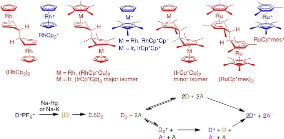
Figure 1. Top) Structures of some organometallic dimers suitable for use as n-dopants and the monomeric cations from which they are synthesized and to which they are converted on reaction with acceptors; Lower left) synthesis of the dimers; and Lower right) mechanisms by which they react with acceptors such as organic semiconductors or electrode surfaces, where D2 denotes the neutral 2 × 18-electron dimer, D+ the corresponding 18-electron cationic monomer, and D the 19-electron neutral monomer.
Indeed, the dimers shown do react with a variety of acceptors to form the corresponding monomer cations and the acceptor anion (or dianion, if the potentials and stoichiometries allow). Whether the C—C bond cleavage precedes or follows electron transfer depends on the dimer and acceptor combination in question.11,12 The reaction of one example with 6,13-bis(tri(isopropyl)silylethynyl)pentacene (TIPS-pentacene, Product No. 716006) is shown in Figure 2.
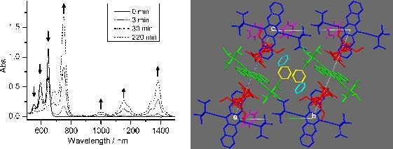
Figure 2. Left) UV-vis. spectra showing the reduction of TIPS-pentacene (Product No. 716006) to its radical anion by ruthenium pentamethylcyclopentadienyl 1,3,5-triethylbenzene dimer (a close analogue of (RuCp*mes)2,) in chlorobenzene solution. Right) View of the crystal structure of the doping product showing organometallic monomeric cations in red, two types of crystallographically distinct TIPS-pentacene radical anions in green and blue, and benzene molecules in yellow, turquoise, and magenta. Reproduced with permission from reference 11 (©2012 Wiley-VCH).
They can be used for the n-doping of materials including fullerenes, perylene diimides, copper phthalocyanine (702854, 546674, and 546682) (Figure 3), and TIPS-pentacene, i.e. materials with solid-state electron affinities (EAs) as low as ca. 3 eV.13,14 The estimated potential, determine their thermodynamic ability to act as reductants, for the reactions:
0.5D2 = D+ + e–
are ca. –1.7 V vs. ferrocene in the case of (RhCp2)2 and ca. –2.0 V for the other examples.12 Since this reaction involves both electron transfer and bond cleavage, these compounds are much more tolerant of air and moisture, and are therefore more easily handled than simple one-electron reductants with similar potentials, such as decamethylcobaltocene (401781, CoCp*2, –1.9 V). The solid dimers can be handled in air (for weighing or for transfer to a vacuum chamber), but are best stored in inert atmosphere. Solutions are also more sensitive to air than the solids, but are considerably more stable than solutions of CoCp*2. Suitable solvents include THF, toluene, and chlorobenzene (all of which should be dried); however, the dimers react with dichloromethane and chloroform. It should be emphasized that while the moderate air stability of the dimeric dopants may be useful for handling the pure dopants, the precautions necessary for handling the resultant doped films (and, assuming rapid reaction with semiconductors, during processing) will generally be dictated by the sensitivity of the reduced semiconductors.
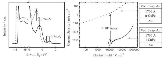
Figure 3. Left) Ultraviolet photoelectron spectroscopy (UPS) spectra of 10 nm evaporated films of undoped CuPc (solid line, Product Nos. 702854, 546674 and 546682) and of CuPc doped with 3.5 wt% (RhCp2)2; the significant shift of the filled levels away from the Fermi level is indicative of n-doping. Right) J-V characteristics of simple sandwich structures based on undoped CuPc and CuPc doped with 5 wt% (RhCp2)2 showing the dramatic effects of doping on conductivity. Reproduced with permission from reference 14 (©2012 Wiley-VCH).
Organic semiconductors can be n-doped with the dimers through co-sublimation or through reaction in solution prior to spin-coating. Controlled vacuum deposition of monomeric CoCp2 and CoCp*2 requires specialized equipment,15 the dimers have lower vapor pressures, enabling their use in conventional evaporation crucibles. As well as demonstrating doping through the current-voltage characteristics of simple sandwich devices and ultraviolet photoelectron spectroscopy (UPS) measurements, the dimeric species have also been incorporated into devices. Ultralow doping of OFETs based on unpurified C60 has been shown to largely compensate for the charge-trapping effects of defects, resulting in a reduction in the threshold voltage to a value comparable to that obtained using highly purified C60 (572500), as shown in Figure 4, while retaining a high current on-off ratio (>105).16 In another study, heavy doping of a C60 transistor in the immediate vicinity of the source and drain electrodes was shown to reduce the contact resistance and, therefore, increase the effective field-effect mobility, while retaining useful on-off ratios.17
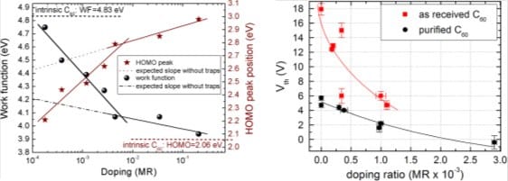
Figure 4. Left) Effects of different levels of doping on the Fermi level of C60, plotted both as work function (WF) (i.e., vs. vacuum) and as the position relative to the onset of ionization from the C60 HOMO. The regimes of strong dependence of the Fermi level position on doping level are attributed to trap filling, while the shallower regions are attributed to contribution of free carriers. Reproduced with permission from reference 18 (©2012 American Physical Society). Right) Effect of ultralow doping with (RuCp*mes)2 on the threshold voltage of OFETs fabricated with two batches of C60 with differing purities. The on/off ratios for all but the most heavily doped device are all 105 or higher. Reproduced with permission from reference 16 (©2012 AIP Publishing LLC).
In addition to their use as dopants for semiconductors and surfaces (see below) the reducing strength and stability of these dimers, coupled with the stability of the resulting monomer cations, may make them convenient reagents for generating reduced species for other applications. For spectroscopic studies in solution the cations are colorless and diamagnetic.
Molybdenum Tris(dithiolene)s as p-Dopants
2,3,5,6-Tetrafluoro-7,7,8,8-tetracyanoquinodimethane (376779, F4-TCNQ, E1/2(red) = +0.15 V vs. ferrocenium/ferrocene in CH2Cl2;19 solid state EA = 5.2 eV20) is one of the most widely used p-dopants for organic semiconductors. It is highly volatile (making controlled sublimation challenging), poorly soluble, and prone to diffusion in some host materials. With some semiconductors, significant donor-acceptor orbital overlap precludes an integral electron-transfer reaction.21
The recent introduction of the more three-dimensional molybdenum tris(1,2-bis(trifluoromethyl)ethane-1,2-dithiolene, Mo(tfd)3 (795712, Figure 5)22,23 – a long-established one-electron oxidant that has been used in synthetic organometallic chemistry24 – as a p-dopant helps address some of these drawbacks. It can be readily evaporated in standard vacuum deposition equipment and has been co-sublimed with organic semiconductors including a-NPD (765015),19,25 pentacene (698423 and 684848),26 and CuPc (702854, 546674 and 546682),14 to give n-doped films. The Mo(tfd)3– anion has been found to show stability with respect to diffusion in a-NPD at temperatures of up to 110 °C.25 Mo(tfd)3 has been applied in pentacene OFETs; heavy p-doping of a pentacene OFET in the vicinity of source and drain electrodes was found to reduce contact resistance in similar way to the contact n-doping of C60 described above.26 The “remote doping” of a pentacene OFET, in which the dopant is located within an adjacent a-NPD layer, has also been demonstrated.27
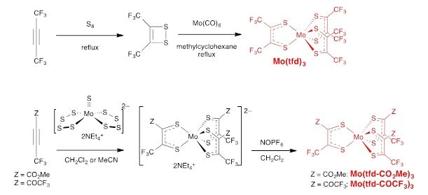
Figure 5. Synthesis of Mo(tfd)3 and more soluble analogues.
Although Mo(tfd)3 has reasonable solubility in organic solvents, its doping products are not always very soluble in solvents suitable for spin-coating of semiconductor films. For example, attempts to dope the archetypal OPV polymer P3HT at all but ultralow doping levels led to the very rapid formation of precipitates. Accordingly more soluble analogues molybdenum tris-(1-(methoxycarbonyl)-2-(trifluoromethyl)ethane-1,2-dithiolene), Mo(tfd-CO2Me)3, and molybdenum tris-(1-(trifluoroacetyl)-2-(trifluoromethyl)ethane-1,2-dithiolene), Mo(tfd-COCF3)3, were developed for solution p-doping of semiconductors (Figure 5, Table 1). P3HT doped with 4 wt% Mo(tfd-CO2Me)3 has been found to be an effective hole-collecting contact for organic photovoltaics that is processible from organic solution (Figure 6),28 while Mo(tfd-COCF3)3 has been used in solution-processed field-effect transistors based on p-doped TIPS-pentacene / polymer blends.29
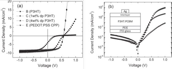
Figure 6. Left) J-V characteristics for bulk heterojunction OPV devices under AM1.5 illumination and Right) in the dark where the interlayer is either P3HT (B), P3HT p-doped with Mo(tfd-CO2Me)3 (C and D), or PEDOT:PSS (E). Note the similarity of the data for D and E. Reproduced with permission from reference 28 (©2013 Wiley-VCH).
All three of these p-dopants are air stable in the solid state. They are soluble in solvents such as dichloromethane, chlorobenzene, and toluene; these solutions, however, slowly decompose on exposure to air, presumably through reduction by water. The compounds are incompatible with more Lewis basic solvents such as THF, acetonitrile, and acetone, in which they are reduced or otherwise decomposed.
Applications to Surface Doping
Some of the dimeric n-dopants discussed here have been used for surface doping, both using immersion in toluene solutions and by sublimation onto substrates. The work functions (WFs) of indium tin oxide (ITO), ZnO, and Au can all be significantly lowered.30 Thus, ITO can be rendered an effective electron-injecting electrode. The WF reduction is particularly dramatic when dopant is sublimed onto a single-crystal of ZnO.31 In all cases, the major origin of the WF change is the interface dipole formed by the partial monolayer of dopant-derived monomeric cations on the negatively charged electrode material.
When applied to monolayer graphene32 the WF change has significant contributions from both population of the graphene conduction band and the interface dipole. Moreover, the conductivity of the graphene is significantly increased, with only minimal effects on its transparency. Graphene has also been p-doped using Mo(tfd-COCF3)3, leading to increased conductivity, but to significantly increased WF.32 Thus, using n- and p-dopants, the WF of graphene can be tuned over a range of ca. 1.8 eV as shown schematically in Figure 7. In principle, similar effects should be possible on other 2D materials; indeed, a dopant based on the dimer of an organic radical, but with similar reactivity to the organometallic dimers described here, has recently been used in the n-doping of large-area trilayer MoS2.33

Figure 7. Schematic showing effects of n- and p-doping of graphene with metal-organic dopants based on data from reference 32.
Summary
The dimers of group-9 metallocenes and of RuCp*mes are versatile and powerful n-dopants that are relatively easily handled and can be applied to doping both organic semiconductors and surfaces using either solution or vacuum processing. Molybdenum tris(dithiolene) complexes are a similarly versatile family of p-dopants.
Materials
References
To continue reading please sign in or create an account.
Don't Have An Account?