Graphene-Based Transparent Conductive Electrodes
Introduction
A transparent conductive electrode (TCE) is an essential component of various optoelectronic devices such as solar cells, liquid-crystal displays (LCD), light-emitting diodes (LED), and touch screens. The most commonly used TCEs are doped metal oxide-coated glasses, e.g., tindoped indium oxide (ITO), fluorine-doped tin oxide (FTO), and aluminum zinc oxide (AZO). However, metal oxide materials have several shortcomings that limit their usage by current industry and for future electronics. One major issue is the scarcity of the indium supply and the resulting increasing costs. In addition, ITO, together with its substitutes FTO and AZO, is brittle and thus unsuitable for applications in flexible and stretchable electronic devices.
Emerging materials for fabricating TCEs include carbon nanotubes (CNTs), nanostructured metals (e.g., metal grids and metallic nanowires), and graphene (Figures 1A–C). It is generally accepted that substitute TCEs must have a sheet resistance of RS<100 Ω/sq. coupled with transmittance T>90% in the visible range. Large-area display and large-area solidstate lighting are even more demanding, with requirements of a sheet resistance below 5 Ω/sq. A CNT network is severely limited by the large contact resistance of tube–tube junctions and, therefore, is still far from practical applications. A random network of Ag nanowires (AgNWs, Prod. Nos. 778095, 739421 and 739448) can lead to an optoelectronic performance of 10–20 Ω/sq. with 90% optical transparency.
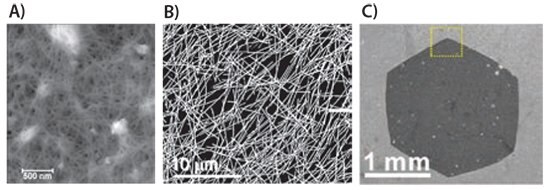
Figure 1. A) AFM image of a CNT network10. B) SEM image of an AgNW network9. C) SEM image of a graphene flake11.
Graphene is a single layer of sp2 carbon atoms bonded in a honeycomb lattice. Graphene has remarkable properties:
- Intrinsic electron mobility (2×105 cm2/V∙s) enables high electrical conductivity.
- High thermal conductivity (~5×10³ W/m∙K) can dissipate heat generated in power electronics.
- High mechanical strength can meet the need of flexible electronics.
- Chemical stability makes graphene useful in harsh environments.
Graphene is transparent starting from the entire visible region through the far infrared. The minimum sheet resistance of an ideal undoped single-layer graphene (SLG) is about 31 Ω/sq. (free-standing single-layer graphene with room temperature mobility of 2×105 cm2/V∙s and carrier concentration of 1012 cm-2), which makes graphene a promising material for TCE applications. A p-doped monolayer graphene (Prod. No. 773719) shows 600 Ω/sq. for T>97%. Coleman et al. predicted an upper limit RS of undoped graphite film, e.g., few-layer graphene (FLG) at 337 Ω/sq. for T=90%. This is far below the minimum requirement for industrial use since the intrinsic carrier concentration in graphene is low. However, for highly doped graphene RS can be reduced to 62.4/N Ω/sq., where N is the number of graphene layers in the film. The theoretical transmittance of a free-standing graphene can be derived using Fresnel equations, giving T=100–2.3N (%) depending on the number of layers N. The absorbance per layer of graphene can be calculated as A=1–T=2.3%. Therefore, four-layer graphene will result in an RS of 15 Ω/sq. and T~90%, sufficient for most transparent conductor applications.
This article presents a brief summary of recent research on graphenebased TCEs. We discuss the use of graphene made using wet chemical methods and in gas phase and compare the advantages and disadvantages of each technique. The combination of graphene with other nanomaterials is also highlighted because of the excellent performance of the resulting TCEs. An outlook on the future development of graphene-based TCEs is also provided.
Fundamentals
The crucial requirements for a TCE are high electrical conductivity and high optical transparency—very often a trade-off since electrical conductivity and optical transparency are oppositely controlled by the film thickness. Furthermore, the intrinsic properties of a material also limit the overall performance of a TCE. The transport in a solid-state conductor states that the DC conductivity σDC is proportional to the carrier concentration n (electron or hole), while optically, the classical Drude theory teaches that the plasma frequency (material’s cutoff frequency in the optical transmittance spectrum) is proportional to the square root of n. This means that optical transmittance is sacrificed when improving the DC conductivity by increasing n. Explicitly, an ideal TCE is low in n and high in carrier mobility. On this basis, graphene is a unique TCE material that combines high electron mobility and low carrier concentration due to its outstanding two-dimensional electron gas. Assuming a lightly doped graphene with free electron concentration (n~1019 cm-3 or 1013 cm-2, eight or nine orders of magnitude lower than semiconductors or metals), the plasma wavelength is well shifted to far-infrared. However, with the high mobility of graphene (~104 cm2/V∙s at room temperature), the DC conductivity is still considerably high.
Another issue for optimizing TCE performance is that the (RS, T) pair cannot be compared directly for different TCEs. Aside from the carrier concentration n and carrier mobility μ, the (RS, T) of TCEs are primarily affected by the film thickness t. Therefore, an intrinsic measurement is needed for direct and accurate comparison of different materials at various thicknesses. For easy comparison, a recent study suggests a figure-of-merit (FOM). Note that the sheet resistance of a conducting film is physically linked with its transparency. The sheet resistance is determined by DC conductivity σDC.

The transmittance is controlled by optical conductivity σOP by

where Z0=377 Ω is the impedance of free space. A combination of Equations 1 and 2 can eliminate the film thickness t and gives

The (RS, T) pair is, therefore, only determined by the conductivity ratio (Equation 4). A high FOM will result in the desired TCE with a high T at a low RS

The minimum industrial requirement (100 Ω/sq., T=90%) can now be translated into FOM>35 using Equation 4. ITO has an FOM generally falling into the range 35–260 (Prod. Nos. 703192 and 703184: 8–60 Ω/sq., T=84%). As mentioned before, well-doped graphene can possess RS=62.4/N Ω/sq. for T=100–2.3N (%) varying with the number of layers N, which results in FOMs ranging from 244 (4-layer) to 258 (single-layer). Although the FOM is a semi-empirical approach (T at 550 nm and neglecting the substrate contribution), it offers sufficiently high accuracy and facilitates the comparison among various TCEs.
We also compared graphene-based TCEs from the literature with those industry standards on the basis of FOM. In order to calculate FOMs of TCEs in the literature, sheet resistance, and optical transmittance are extracted and fitted using Equation 3. Data from the literature, together with the calculated FOM, are plotted in Figure 2 and summarized in Table 1.
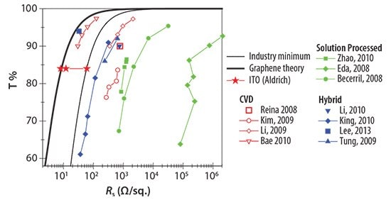
Figure 2.Transmittance and sheet resistance data reported in the literature. These are graphene films prepared by CVD (open red), solution processed graphene (solid green), and hybrid graphene film (solid blue). The red stars represent commercially available ITO. The dashed line illustrates the minimum industry standard for TCE (FOM=35). The solid line corresponds to the calculated case of highly doped graphene (FOM=244).
Solution-processed Graphene TCE
The solution process is likely the most suitable way to make large-scale TCE at the lowest cost. This technique is similar to that used for fabricating CNT TCEs. Typically, the solution process is divided into two steps: 1) breaking the graphite down to graphene flakes, and 2) fabricating the graphene thin film on substrates. Chemical exfoliation and ultrasonic exfoliation are mature techniques for the first top-down step in the solution phase. After purification (centrifugation), either the chemically converted graphene oxide (GO, Prod. Nos. 763705 and 777676) or the sonically cleaved graphene flakes can form a stable suspension in the liquid phase, although the latter usually needs the assistance of a surfactant. The subsequent bottom-up fabrication includes filtrationtransfer, the Langmuir-Blodgett film technique, spin-coating, a liquid-air interface self-assembly, and rod coating. Note that relatively large sheet resistances of solution-processed graphene sheets arise from numerous small-sized grains and grain boundaries. A random network of solution-processed graphene flakes usually exhibits FOM<0.7 (with respect to a few hundred nm in lateral size), according to Coleman’s survey. The small FOM is due to the inter-flake junctions that are analogous to those of nanotube networks.
Chemical exfoliation of GO is accomplished by oxidizing inexpensive graphite powders using strong oxidants, and separated flakes are obtained by subsequent gentle exfoliation. A stable and clear aqueous GO suspension is obtained by washing, filtering, centrifuging, and re-dispersing in water. The GO is surface-functionalized with a high coverage of oxygen-containing groups and is, therefore, insulating. After coating on substrates, the GO thin film needs to be further converted to reduced graphene oxide (rGO, Prod. No. 777684) for electrical conduction (Figure 3A). Technical details about oxidization and reduction were reviewed in a recent article. GO flakes are usually small, most with an area on the order of 100 μm2, because of the unavoidable breaking of GO sheets during the vigorous oxidation. Increasing rGO sheets to 7,000 μm2, Cheng et al. reported a TCE with 840 Ω/sq. at 78% transmittance (FOM=1.8, Table 1). Although many efforts have been devoted to developing a reduction technique, none can fully reduce GO and restore the exact graphene structure. Without the removal of structural defects, the performance of solution-processed TCEs will hardly lead to further breakthroughs.
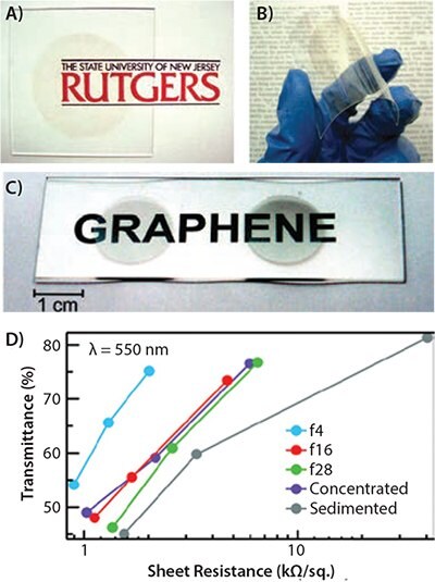
Figure 3.Thin films of solution-processed GO. Photographs of GO thin films on glass (A) and plastic (B) substrates18. C) Photograph of two sorted graphene transparent conductive films on glass. D) Transmittance of graphene transparent conductors produced from different solutions as a function of their sheet resistance at a wavelength of 550 nm39.
Avoiding oxidization and reduction, some direct liquid-phase methods were developed to produce pristine graphene. Coleman et al. pioneered the liquid-phase exfoliation of pristine graphene from bulk graphite with the organic solvents N-methylpyrrolidone (NMP, Prod. No. 328634), N,N-Dimethylacetamide (DMA, Prod. No. 185884), γ-butyrolactone (GBL, Prod. No. B103608), and 1,3-dimethyl- 2-imidazolidinone (DMEU, Prod. No. 40725), which are known to exfoliate CNTs. Blake et al. simply exfoliated graphite by sonication in dimethylformamide (DMF, Prod. No. 227056) and obtained a well-dispersed suspension. Green et al. prepared graphene by ultrasonication of graphite in water with the assistance of the planar surfactant sodium cholate. With density gradient ultracentrifugation, they isolated graphene sheets with controlled thickness (Figure 3A). However, these techniques cannot yet bypass the limitation of grain boundaries (Figure 3C). TCEs with FOM>0.7 in this category are rarely reported.
CVD Graphene TCE
Chemical vapor deposition (CVD) growth appears to be the most suitable approach to fabricate high-performance graphene film. Graphene growth with CVD on transition metal (mainly Ni and Cu) catalytic substrates results in a quality close to that of micro-mechanically exfoliated graphene from highly oriented pyrolytic graphite (HOPG); it readily forms a large-area thin film. Compared with the solution-processed graphene, the CVD graphene is primarily grown in a vacuum and can be costly. However, a reduced cost can be expected in scale-up production since low pressure CVD is compatible with the modern microelectronics industry.
Precursory research on graphene growth on a polycrystalline Ni film was reported by Kong’s group and Hong’s group. The as-grown graphene film can be transferred to glass or plastic substrates by a poly[methyl methacrylate] (PMMA, Prod. Nos. 182230, 182265, 200336, and 445746) or polydimethylsiloxane (PDMS, Prod. Nos. 423785, 482064 and 482145) layer or just left on the PDMS surface as a flexible/ stretchable film (Figure 4A). The resulting TCEs yield (770–1,000 Ω/sq. T=90%)20 and (280 Ω/sq., T=76%), which are equivalent to FOM=3.5–4.5 and 4.1, respectively. Alternatively, graphene TCE derived from CVD on Cu foil (Prod. No. 773697) with a similar transfer technique has better performance than that from the Ni foil and can exhibit (350 Ω/sq., T=90%), e.g., FOM~10. The reason for the higher FOM with Cu is that the as-grown graphene is almost homogeneously single layer, while on Ni the graphene film has not only multiple layers but also variations in the number of layers. Therefore, the charge carrier mobility is seriously affected by inhomogeneity (Refs. vs.).
A quick observation shows the FOM of CVD graphene is one order of magnitude higher than solution-processed graphene. This is also evidenced by Coleman’s survey (FOM~10 for CVD graphene vs. ~0.7 for solution-processed graphene). An immediate cause for the higher FOM is fewer structural defects in CVD graphene, which has been confirmed by micro-Raman spectroscopy numerous times in the literature. The Raman spectra of CVD graphene are almost identical with those of micromechanically exfoliated graphene from HOPG, whereas the solution-processed graphene (especially rGO) has an immortally high D peak indicating a large number of defects. A second contributing factor is the relatively large grain size for CVD graphene (several to tens of microns in lateral size) compared to the solution-processed ones (submicron in lateral size). Research shows a higher charge mobility with increasing graphene grain size, and it can be as high as 10,400 cm2/V∙s for millimeter-size graphene. TCEs fabricated with large-grain-size CVD graphene produce a considerably higher FOM when properly doped.
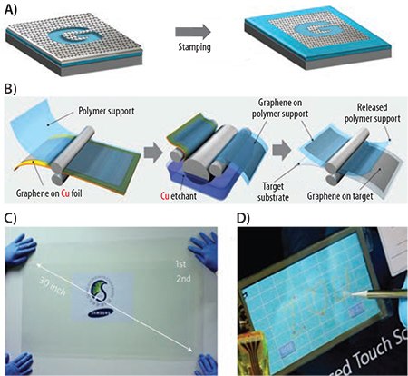
Figure 4. A)Synthesis of patterned graphene films on thin nickel layers and transfer to substrate (reproduced with permission from Ref. 21, copyright 2009 Nature). B) Schematic of the roll-based production of graphene films grown on a copper foil. C) A transparent ultra large-area graphene film transferred on a 35-in. PET sheet. D) A graphene-based touch-screen panel connected to a computer with control software. (B–D are reproduced with permission from Ref. 23, copyright 2010 Nature.)
A breakthrough toward real industrial-level TCE was demonstrated by large-area graphene growth on Cu foil and then transferring it to polyethylene terephthalate (PET) film using a roll-to-roll technique. The results, displayed in Figure 4, show the roll-to-roll transfer of a graphene film grown on a flexible 30-in. PET substrate (Figures 4B and C). The authors demonstrated a large-area touch screen with the transferred graphene and claimed excellent optoelectronic performance over the entire substrate. With a four-layer graphene (repeatedly transferred, p-doped), the TCE exhibits (30 Ω/sq. T=90%) and a calculated FOM=118. These graphene-based TCEs already outperform ITO in some aspects and, therefore, make CVD graphene very promising for practical applications. More technical details about CVD growth of graphene and transfer are summarized by some excellent review articles and are beyond the scope of this paper.
Graphene-based Hybrid TCEs
One method to improve the conductivity of solution-processed graphene films is to incorporate a conductive filler material into them. Recently, some reports have emerged showing the benefits of incorporating CNTs into a matrix with graphene (Tung et al.) mixed GO and CNT in anhydrous hydrazine (Prod. No. 215155) and spin-coated it on glass substrates (Figure 5A). After SOCl2 (thionyl chloride, Prod. No. 447285) doping, the TCE presents 240 Ω/sq. T=86%, equivalent to FOM=10 (Figures 5B–C). A hybrid of CNT and CVD graphene results in 735 Ω/sq. T=90%, which yields FOM~4.7. Using this hybrid film as a top electrode of an Si-based solar cell showed a power conversion efficiency of 5.2%.
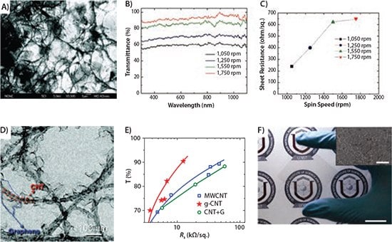
Figure 5. A)An SEM image of a solution-processed graphene-CNT hybrid film. B) Optical transmittance of the solution-processed graphene-CNT films as a function of different spin speeds. C) Sheet resistance versus different spin speeds (A–C reproduced with permission from Ref. 24, copyright 2009 American Chemical Society). D) TEM image of graphenated CNT (g-CNT) and E) its improvement on T% versus RS compared with a physical mixture of graphene and CNT (reproduced with permission from Ref. 47, copyright 2011 American Chemical Society). F) Photograph of graphene−AgNW hybrid film on a PET substrate. The scale bar indicates 2 cm. The inset shows an SEM image of this hybrid (scale bar, 5 μm) (reproduced with permission from Ref. 27, copyright 2013 American Chemical Society).
It is generally accepted that graphene and CNTs (or other filler material) mutually offer conduction pathways in a percolation network. However, the real role of mixing is still under debate since each component can introduce additional tube–flake junction resistance. One study argued the addition of graphene into a single-walled carbon nanotube (SWCNT) network cannot improve the FOM unless the hybrid is SOCl2-treated. More importantly, FOM changes non-monotonically with the film composition; the FOM peaks at 3% wt. graphene (40% higher than the nanotube-only film) and will decrease with more graphene content.26 Yu et al. reported that covalently bonded CNT and graphene (known as graphenated CNT, i.e., g-CNT) can minimize the tube–flake junction resistance. The graphene grown on the sidewall of a CNT with a plasmaenhanced chemical vapor deposition (PECVD) is inherently different from the physical mixture (Figure 5D). The g-CNT can result in an FOM 44% higher than the CNT-only film and 64% higher than the physically mixed CNT-graphene film (Figure 5E).
Another approach to high-performance TCEs is the hybrid of graphene and metallic nanowires. A recent report shows that an AgNW-graphene film (Figure 5F) exhibits an FOM as high as 182 (33 Ω/sq. T=94% at 550 nm). It is not surprising that the AgNW network has a high intrinsic conductivity; however, the graphene layer above or below the AgNWs introduces additional benefits. First, the graphene layer can dissipate heat and electrical stress and, thus, provides strong robustness against electrical breakdown. Second, the graphene layer covering AgNWs preserves TCE’s electrical properties against thermal oxidation.
Conclusion and Outlook
Will ITO eventually give way to graphene for TCEs? Although it is impossible to predict the future at this point, significant progress has been made in the past few years to improve the FOM of graphenebased TCEs from <1 to >100. This has been accomplished by increasing the grain size and crystallinity, reducing defects, appropriate doping, and hybridizing with nanowires/nanotubes. Some recent progress in graphene research may spark further improvement in TCEs. For example, direct growth of graphene on dielectric substrates is one of the most interesting areas of research. Also, rapid progress made catalyst-free growth possible. PECVD techniques enable low-temperature growth of graphene on SiO2/Si (550–650 °C), which can be compatible with the existing infrastructure of the microelectronics industry. A recent study demonstrated direct growth of graphene on dielectric substrates at 400 °C by sophisticated control of a hydrocarbon+H2 plasma to balance etching and nucleation. With this initial success, it is anticipated that direct growth of graphene on plastic substrates will become a reality—an ultimate goal of graphene TCE.
Acknowledgments
Financial support for this work was provided by the U.S. Department of Energy (DE-EE0003208) and the U.S. National Science Foundation (ECCS-1001039).
Materials
References
To continue reading please sign in or create an account.
Don't Have An Account?