Advancements in Quantum Dot Solar Cells
- Introduction
- Nanomaterial Synthesis
- Chemical Synthesis of Nanocrystals
- Classification of Semiconductor QDs Based Solar Cells
- Challenges Ahead and Future Scope
- Conclusion
Introduction
Nanomaterials (NMs) are a class of materials attaining remarkable attention in several research areas due to their tunable physical, chemical, and biological properties. NMs exhibit superior electronic, optical, and chemical characteristics in comparison to their bulk counterparts due to their enhanced surface to volume ratio and the quantum confinement effect. Among NMs, quantum-dots (QDs) are one of the most fascinating, as they show improved optoelectronic properties by the “quantum confinement effect”. QDs have tremendous applications in photovoltaic cells, transistors, LEDs, lasers, photodetectors, quantum computing, and biological imaging.1,2
Quantum dots are based on the theory of quantum confinement, which comes into play when the diameter of the nanoparticle is of the order of the electron’s wavelength. Whenever the particle’s dimension reaches this critical size, the electronic and optical properties of that nanoparticle substantially deviates from its bulk counterpart. In the quantum confinement effect, the particle behaves as a free particle when the confinement dimensions are large as compared to the wavelength of the particle. At this state, the bandgap remains at its original energy due to a continuous energy state. However, when the confining dimension decreases and a specific size limit has been achieved by the particle, the continuous energy state spectrum changes to a discrete energy state spectrum. Resulting in the bandgap dependency on the size of nanoparticle becomes more prominent, as shown in Figure 1. The spectrum of colors in quantum dots relies on this energy, as the size of the quantum dot increases, this results in a red-shift (lower energy), and as the size decreases, there is a blue-shift (higher energy) as shown in Figure 2. In short, quantum confinement is the reason for the increase in the energy difference between bandgap and energy states. In Figure 1, the band structure of bulk semiconductors absorbs light (photons) having > energy bandgap (Eg). In the case of semiconductor cells, photo-generated carriers thermalize to band edges (within about 10−13 s) as excess energy is lost as heat, reducing output. This limitation reduces current, while the thermalization reduces the voltage. As a result, semiconductor cells suffer a trade-off between voltage and current, which can be in part alleviated by using multiple junction implementations.
Figure 1.Energy-Band diagram of semiconductor bulk and nanomaterials.
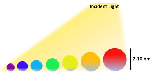
Figure 2.Representative quantum-dots of a particular wavelength.
However, in the case of quantum dots, the QD absorption (bandgap) can be tuned to match incident light and extract carriers without loss of voltage due to thermalization. Thus, solar cells that incorporate QDs may lead to more efficient lightharvesting and energy conversion.
QD based photovoltaic cells have also emerged tremendously in recent years as QDs have the potential of enhancing the power conversion efficiency (PCE) of the photovoltaic devices (PV) beyond the traditional Shockley and Queisser limit, which is 32% in case of Si-based PV cells.3,4 Semiconductor QDs used in PV devices offer serval advantages as light harvesters. First, their size-based quantum confinement enables us to tune their optical response. Furthermore, these QDs offer ways to make use of the hot electrons or to generate multiple charge carriers from a single photon.5 However, limitations of the QDs based PV cells are the potential for defects, which leads to undesirable recombination and hence, limits the PCE of the resultant device.
Various strategies have been suggested by researchers to overcome these issues. Our review provides a brief overview of efficient QDs, synthesis, strategies for designing QDs based PV cells, shortcomings, and suggestions to overcome the drawbacks that limit efficiency. This review covers the significant aspects of QD solar cells (QDSCs), which are essential to understand to improve this field and its commercialization further.
Nanomaterial Synthesis
Nanomaterials can be synthesized using various techniques, including both physical and chemical methods; both are described below. The physical methods include techniques such as gas condensation, chemical vapor deposition, atomic layer deposition, and pulsed laser depositions. The chemical methods, such as heat-up technique, hot-injection technique, re-precipitation method, and hydrothermal synthesis, are also discussed. Each of these methods has advantages and disadvantages for synthesis.
Gas Condensation
In this technique, the vaporization of a metallic or inorganic precursor material occurs using thermal evaporation in 1–50 m bar atmospheric pressure. The formation of fine particles with a dimension of 100nm by the collision of evaporated atoms with residual gas molecules results from ‘gas evaporation’.
Vacuum Deposition Process
Another commonly used physical technique in which the deposition of compounds/alloys occurs in a vacuum after vaporization. The process requires an ambient pressure <0.1m bar via gas to provide collision and cooling for nucleation, resulting in particles or clusters in the range of 1–100 nm.
Chemical Vapor Deposition (CVD) and Chemical Vapor Condensation (CVC)
The CVD process involves a chemical reaction between volatile precursors and the surface of the materials to be coated. In CVD, a precursor gas(es) a flowed into a chamber containing one or more heated objects required to coat. The chemical reactions occur near hot surfaces, resulting in the deposition of a thin film on the surface. CVD has relatively high deposition rates but requires volatile precursors and elevated temperatures, limiting its applicability for wide range of materials.
Pulsed Laser Deposition (PLD)
Pulsed laser deposition uses a high-power pulsed laser beam, which is focused on a target of the material that is to be deposited. The process happens in a vacuum chamber, where the vaporized target material (in a plasma plume) is deposited as a thin film on a substrate.
Mechanical Attrition or Ball Milling
Another physical technique that produces nanostructures by the structural-decomposition of coarser grain-structures resulting from plastic deformation is mechanical attrition or ball milling.
Chemical Synthesis of Nanocrystals
Heat-Up Technique
The heat-up technique is a non-injection method in which the precursor is heated steadily in the presence of ligands. To perform this technique, mix the required precursors at room temperature, and then increase the heat to the suitable growth temperature. Most of the heat-up synthesis techniques deliver polydisperse particles due to the random nucleation that occurs over different time scales. Copper Indium Sulphide (CIS) QDs are generally synthesized using this method for applications in PV devices.
Hot-Injection Technique
In this technique, a room temperature precursor solution is injected into a hot reaction medium in the presence of suitable surfactant molecules. The precursor solution initiates monomer formation, and due to their supersaturation, causes nuclei formation. After the injection of room temperature precursor, the reaction temperature reduces and the precursor solution is quickly reacts with remaining precursor causing the prevention of further nucleation. Overall, the growth of nanocrystals occur at lower temperature than nucleation’s temperature. This temperature decrease creates an energy barrier for nucleation, resulting in uniform-sized particles of the desired material. The synthesis of highly luminescent CdSe nanocrystals using this technique occurs by injection of a room temperature solution of precursor molecules into hot (300 °C) trioctylphosphine oxide (TOPO).
Ligand Assisted Reprecipitation Method
Ligand-assisted re-precipitation (LARP) technique is an efficient method for the synthesis of organometal halide perovskite nanocrystals (PNCs). Zhang et al. initially introduced the LARP approach for the synthesis of MAPbX3 NCs.6 In this method, the preparation of an initial solution occurs by adding the lead halide and organic halide salt precursors into a polar solvent such as dimethylformamide dimethylformamide (DMF) or Dimethyl sulfoxide (DMSO) in the presence of ligands such as octylamine and oleic acid. Then, the dropwise addition of this solution into a non-polar medium (such as toluene). Figure 3 shows the schematic diagram for the synthesis. The miscibility gap between both solvents initiates the recrystallization of lead halide perovskite NCs. After the formation of nanocrystals, the purification needs to be carried out at high RPM (2 times) using a centrifuge machine. LARP method is viable for industrialization and scalability purpose. While LARP method offers an economical route to prepare high quality nanocrystals; it still hamper the precise control of reaction conditions in contrast to hot-injection route. Overall, less control on shape and size of nanocrystals is an issue in LARP method.

Figure 3.Schematic diagram showing the ligand-assisted re-precipitation (LARP) method.6
Hydrothermal Synthesis
This technique finds use in the synthesis of nanocrystals of different chemical compounds in a closed system such as an autoclave, that can withstand high temperature and pressure over time. All the physical and chemical processes in the autoclave occur at temperatures above 100 °C and pressures above 1 atm. The hydrothermal technique allows for the synthesis of zeolites, QDs of various oxides and carbon, and various luminescent perovskites.
Classification of Semiconductor QDs Based Solar Cells
CdSe (Cadmium Selenide)
CdSe is a well-known semiconducting material consisting of a direct band of 1.74 eV at room temperature, belongs to the II-VI group of semiconductors, and highly favors wide range optical absorption in the visible range. Most of the earlier research extensively focused on the synthesis of CdSe nanocrystal, especially with the synthesis of QDs due to ease of bandgap tunability with controlled size growth.7,8 The outstanding fluorescence of CdSe materials make them ideal for use in various light-harvesting applications, especially photovoltaics. S. N. Sharma et al.9 demonstrated a photoinduced charge transfer between CdSe QDs and p-phenylenediamine (ppd). They found that the formation of ppd cation radicals and other charged species at the surface extends the bleaching recovery over several microseconds. To facilitate carrier injection and lightabsorption in QD solar cells, the energy levels of quantum dots should match appropriately, as seen in the cases of CdS/CuInS2, CdSe/CdTe and CdS/CdSe10,11 core/shell QD structures. The CdS/ CdSe core/shell structure is one of the most widely explored QD structure owing to its easy synthesis, high stability with an efficiency (PCE) ~ 5%. Currently, the highest performing QD solar cells exhibit a PCE of only 6–8% due to the severe chargerecombination and low photoanode area coverage. To encounter this situation, mesoporous photoanodes required to employ to enhance electron transport and large area acquisition. The best performing QD solar cells contain TiO2 as a mesoporous photoanode because of its low-cost and excellent chemical stability. Linkers, such as MPA-mercaptopropionic acid, have also been used for TiO2 film coating, followed by exposures to QDs for QDSC assembly.12
InP (Indium Phosphide)
InP (group III–V) is one of the most promising materials for photovoltaic applications, with an appropriate band gap (1.35 eV), higher mobilities, and a high absorption coefficient. InP shares the lowest intrinsic toxicity as compared to Cadmium based cells. The use of different capping ligands help to overcome the size effect and bandgap tunability. Highly luminescent InP QDs with a bluish-green emission (λ~490 nm) has been reported by synthesis using the hot injection technique, with trioctyl phosphine (TOP) as the source of P instead of the conventional but toxic and expensive tristrimethylsilyylphosphine (P(SiMe3)3) without resorting to any post-synthesis etching to tune the emission to the blue region.13 InP QDs are attractive due to their higher photostability and their strong covalent bond. Due to these properties, InP is one of the favorite materials for use in QDSCs. Although the strong covalent bond may cause complications for monodisperse nanoparticle synthesis, which in turn produces defects and cause a lower luminescence efficiency, to overcome the stability situation, modification to time, temperature, and choice of ligands is crucial. Other disadvantages of InP include low photocurrent due to the electron loss at the QD-electrolyte interface, which requires QD loading with enough surface area utilization in a broad range of visible spectra. Furthermore, the size of the QD can be tuned to increase the light-harvesting range. While doping can be useful for tuning the QD to the visible spectra.13,14
PbS (Lead Sulphide)
PbS QDs are a promising nanostructured material for photovoltaic applications. PbS is known as a photo absorber in the visible and near infra-red regions, due to its bandgap tunability and solution processability and is also considered a low-cost solution-processed photovoltaic material. Rapid advancement in quantum solar-cells by architecting and surface modification led to a power conversion efficiency of 11.3% with outstanding stability. However, the ligand exchange process renders the manufacturing of the QD device. The choice of capping ligand (oleic acid, MPA, thiols, etc.) plays a crucial role in the stability of QDs. A typically used capping ligand, oleic acid, both stabilizes and helps to passivate the surface, making it insulated from surrounding QDs. It also allows interdot distance adjustment, which defines the coupling strength between the inter-related QDs.15 An enhanced efficiency of 8.45% was reported for conventionally structured PbS QD solar cells, in which a modified anode buffer layer comprising of a unique conjugated polymer PDTPBT was used. This anode modification improved the device performance due to increased hole extraction to the anode and reduced interfacial carrier recombination which enhanced Voc significantly.16
PbSe (Lead Selenide)
PbSe is one of the reliable colloidal QDs for the next-generation photovoltaics. Previously, PbS QDs were the primary research focus due to their stability under extreme conditions. There is much interest in expanding the work to PbSe QDs, which shows increased photocurrent due to multiple generations of excitons. The synthesis of a range of sizes is required to overcome the stability issues of using PbSe ambient conditions.17 Air stable PbSe QDs were firstly synthesized by the cation exchange method, followed by the solution-phase ligandexchange approach. Then the absorber layers were prepared using the single-step spin coating method, which in turn shows an excellent efficiency of 10.68%, which was nearly 16% higher than earlier recorded data. The stability of that prepared cell remains stable up to 40 days with eight hours of continuous illumination. The performance of PbSe QD solar cells was improved further by introducing SnO2 based buffer layer at the interface ETL/PbSe, and this leads to better extraction of charge carriers. Band alignment between the PbSe QD absorber layer and the TiO2 buffer layer could be attributed to the performance enhancement of the cell.13,18 Figure 4 shows the schematic for the fundamental QD base solar-cell structure.
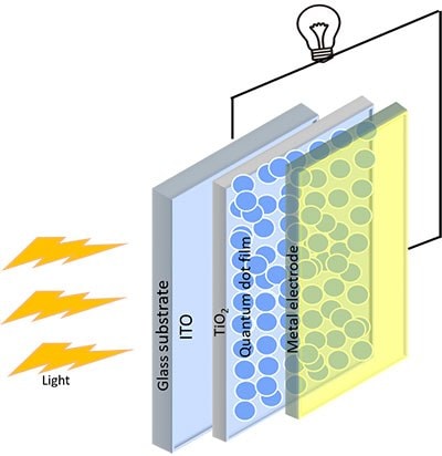
Figure 4.Schematic diagram of a quantum-dot solar-cell.
CIS (Copper-Indium/Selenide)
Copper-indium-selenide (CuInSe2) is a p-type semiconductor that has drawn tremendous attraction in the field of photovoltaic applications due to its wide bandgap (1.04 eV) and significant absorption coefficient with high stability. It is considered an alternative to the cadmium/lead-free toxic elements. In 1976 a CIS solar cell was fabricated, with an efficiency of ~ 5%, using the evaporation technique.19 The parameters of the cell remain stable over a long time, provided the temperature does not exceed 90 °C. Unfortunately, even after many precautions, such as placing the assembly in a glass encapsulation, their life does not exceed more than ten years. Moreover, indium resource limitations are a significant concern.20 The cell efficiency typically depends on the crystalline nature/structure of the material formed and the share of the Indium and Copper element, In the case of CIS, the hole concentration decreases as the concentration of Copper decreases. The efficiency of CIS increased to 7% when introducing CdS as the absorber layer. Both CIS and CdS show low resistivities when deposited by vapor deposition. Further technological improvement in junctions enables the maximum photon absorption and drags the efficiency to 10%.19 Figure 5 shows the Schematic diagram representing CIS based Solar-cell.

Figure 5.Schematic diagram representing a CIS based solar cell.
CIGS (Copper-Indium/Gallium/Selenide)
Several different research technologies emerged, leading to the incorporation of gallium in the CIS cell, also known as CIGS. Following the addition of Gallium (Ga), sodium (Na) has also been incorporated into the absorber layer of CIGS cell assembly with a thin layer of CdS as a buffer layer, which has significantly enhanced the cell efficiency to 22.6%.20–22 CIGS formation follows two-steps, the optimized CIG precursors are deposited onto a substrate; this could be done by sputtering, vapor deposition, or and electrodeposition. In most of CIG (S, Se) deposition, Ink deposition is trending due to the low material utilization, with less waste and ease of preparation. Figure 5 shows the Schematic diagram representing CIS based Solar-cell. Sharma et al. reported an aqueous-free based rapid synthesis (~ 45 mins.) of organically-capped Se-rich CIGSe by the colloidal route.23 They reported a process of purification which elevated the charge-transport between CIGSe nanocrystals for the realization of an efficient photovoltaic device without resorting to sodalime- glass (SLG), harsh chemical treatments, or post-deposition thermal selenization.
However, sputtering has proven to be the most efficient method with respect to the cell efficiency. Ga is required to incorporate into Cu targets since Ga has a very low melting point. Stacking sequences of precursor layers can profoundly influence the elemental distribution through the depth of the final film. Most of the time, some Se has already incorporated by precursor layers, which are, in turn, annealed and selenized. The substrate preparation in CIGS solar cells is the most crucial and tedious process, which plays a vital role in the development of the whole device. Molybdenum deposition onto a flexible/rigid substrate defines the condition of selenization. The annealing temperature challenges the ability to create a flexible, CIGS based device. Flexible substrates cannot withstand this high temperature of 500 °C, which is a mandatory step for absorber layer crystallization in a CIGS cell. The efficiency recorded using a flexible substrate is ~20%. In CIGS structure, the role of n-semiconductor is fulfilled by ZnO as the buffer layer and CdS as the window layer; both can be replaced by each other. A schematic of the CIGS solar cell has a structure of substrate/ Mo/CIGS/CdS/ZnO/metal grid (Figure 6). Here light enters via a Transparent conductive oxide (TCO) and a back-contact deposited on the substrate.24
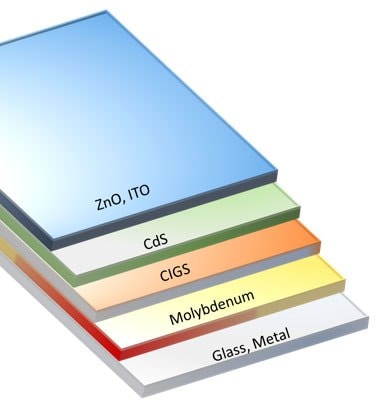
Figure 6.Schematic representing a CIGS solar-cell structure.
Perovskites
Perovskites are a class of minerals with a crystalline cubic/ diamond-like structure. A conventional perovskite is a calcium titanium oxide (CaTiO3) mineral, first found in the Ural Mountains of Russia. The metal halide perovskite, which has a similar structure to oxide perovskites, are potential candidates for solar-cell applications. A halide perovskite has an ABX3 crystal structure (Figure 7), where A is a monovalent cation, such as Cs+, MA+, FA+, B is a divalent cation such as Pb2+ or Sn2+, and X is an anion such as Cl-, Br-, and I-.25
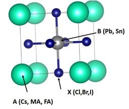
Figure 7.A Perovskite cubic crystal structure25
Perovskites offer several advantages in the solar cell regime. Perovskites offer composition with a tunable bandgap (1.5– 2.3eV), which is the most favorable condition for maximum sunlight absorption and hence the maximum conversion of electricity.26–28 They can be synthesized by solution processing techniques, which makes the fabrication process cost-effective when compared to conventional solar cell technologies.29,30 Perovskites can also be used as an electron/hole transport layer to enhance charge transport. It has high charge mobility, high excitation coefficient, long carrier lifetime, carrier diffusion rate, and high absorption coefficient.31 Furthermore, the formation of perovskite thin films requires very little material. No rare earth elements are required. Perovskites are highly tolerant of defects, which creates a large manufacturing yield.25 The module has the lowest environmental effect, depending upon the manufacturing method used. They can be easily deposited onto a flexible substrate, opening a new area for further research.
The disadvantages of perovskites are their environmental induced (moisture, oxygen, and light) stability issues. However, due to the rapid advancements in cell efficiency, researchers have overcome many of these limitations by providing a standardized packaging assembly. Other stability issues like mechanical durability, thermal influence, applied voltage heating, and current-voltage behavior require further detailed study.
Most efficient metal halide perovskite is composed of lead (Pb) based material, such as, FAPbI3,MAPbI3, and CsPbI3. Figure 8 shows the schematic of a perovskite solar cell. Currently, researchers have achieved very high efficiencies (>25%) with perovskite-based solar cells.32 The National Center of Photovoltaics (NCPV) has shown that when carriers are excited with high energy, the cooling rate in perovskite materials slows down during the cooling process. The cooling occurs more slowly when using MAPbI3 as compared to other traditional and expensive structures, making this material an excellent candidate for next-generation hot carrier solar cells with high efficiency. Since excitons do not remain stable at room temperature, the coulomb interaction between carriers (electrons and holes) dramatically affects the optical absorption in these materials, and the presence of excitons impacts on recombination dynamics.
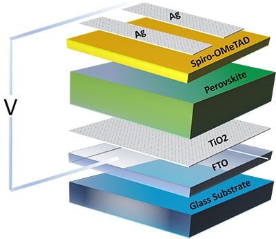
Figure 8.Schematic representing a perovskite solar cell prototype.
Researchers found that even on the non-passivated surfaces, the surface recombination is significantly slower than that of recombination in other non-passivated semiconductors.33 The toxicity of lead in perovskites is a severe threat to the environment; therefore, lead-free perovskite structures have become a driving force in research. The Sn-based perovskites systems studied so far, exhibit poor film morphology and uncontrolled crystallization, which limit the actual potential of perovskites. Although many additives such as SnF2, SnCl2, etc. overcome some of these effects, unfortunately, the stability and efficiency have not been up to current standards of lead-based perovskites. More research is required to address this problem using different permutations and combinations of materials.
Challenges Ahead and Future Scope
In the past few years, QD based PV devices, especially perovskite solar cells, have improved significantly in terms of efficiency, but their stability is still a matter of concern. One possible solution in this direction to improve the stability of perovskite-based PV devices is by minimizing the perovskite dimensionality. The stability of layered 2D films and nanocrystal QDs based PV cells are still better than the perovskite 3D filmbased devices. Also, the QDs of perovskites have better phase stability and composition tunability in comparison to thin-film perovskites. Despite all this, the highest reported efficiency of QDs based device is 13.4%, still much lesser than 25.2% reported for a thin-film perovskite device.35,36 To address the issue of low efficiency, Hao et al., synthesized multi-cation perovskites using the oleic acid (OA) ligand-assisted cation exchange method and they got an enhanced efficiency of more than 16%.31 Surface trap defects also limits the efficiency of QDs based PV cells. To overcome this issue, core-shell architecture based QDs were designed in which a shell of wider bandgap material (CdS) was over-coated around the core (CdSeTe). This architecture minimizes the surface defects and boosts the PCE of the resultant device.32 Similarly, to reduce the charge recombination at the interface of photoanode/electrolyte in QDPV cells, the concept of the passivation layer was introduced. The passive layer deposition minimizes the charge recombination and restricts the movement of electron in the electrolyte, which is one of the reasons for the limited efficiency of quantum dot solar cells (QDSCs).21,37 In spite the previously mentioned measures to improve the stability and efficiency of QDSCs, there are still two significant challenges in the path of their commercialization. The first is the high processing cost of QD materials, and the other is the need for efficient deposition methods for QDSCs fabrication. Hence, efforts are needed to minimize the cost of QD synthesis and device fabrication to ensure better commercialization of QDSCs. Also, the current method for QDSC fabrication relies on the spin-coating technique for the layered deposition of perovskites films, which can’t be scaled up for mass production. Hence, significant research is still required in this domain to resolve the various existing drawbacks in the QDSC technology for the successful commercialization of high-efficiency stable QD PV devices. Lead-free perovskites are also emerging as an environmentalfriendly substitute for lead-based perovskites, but a lot for research is still required to improve their efficiency and stability so that it can match with that of lead-based perovskites.
Conclusion
In this article, we reviewed the recent research in the area of quantum dot solar cells in terms of the QDs synthesis methods, their advantages and disadvantages, literature review of the recently developed QDSCs devices, their architecture, and their efficiencies and shortcomings. We have discussed in detail the working mechanism of several QDSCs, including CdSe, CIS, PbS, PbSe, InP, perovskites, etc. and their highest reported efficiencies to date. Apart from this, we have described the factors responsible for the limited efficiency and stability of the QDSCs and their possible solutions, as suggested by different research groups. The article highlights how the rapidly progressing QD based PV devices are emerging and, in the future could surpass the Si photovoltaics in terms of efficiency and stability.
Acknowledgments
The authors (PS) and (SB) sincerely acknowledge the Council of Scientific & Industrial Research (CSIR), Government of India, for providing Junior Research fellowship (#31/001(521)/2018-EMR-I) and Research Associate fellowship (#31/1(0494)/2018-EMR-I. P.V. acknowledges Presidential Postdoctoral Fellowship, NTU Singapore via grant 04INS000581C150OOE01, and Dr. Dani Metin.
Materials
References
如要继续阅读,请登录或创建帐户。
暂无帐户?