Nanowire Synthesis: From Top-Down to Bottom-Up
Introduction
The properties of many devices are limited by the intrinsic properties of the materials that compose them. However, at the nanoscale, device properties are no longer dependent solely on the material type, but also on material geometry (for example, transforming glass into the brilliant colors of an opal). Nanowires, anisotropic structures with diameters from one to hundreds of nanometers and lengths of tens to hundreds of microns, provide a unique platform for harnessing these nanoscale phenomena.
Many nanowires are single crystals, and as a result of their narrow diameter have an extremely high surface area. This high surface-area-to-volume ratio makes nanowires very sensitive to changes in surface chemistry and gives rise to their prevalence in sensor development.1 Nanowire diameters are also sufficiently small to allow the penetration of biological structures without damage, while their length allows them to transport signals in and out of a cell.1 These properties also make nanowires very effective as battery electrodes, with long conduction pathways that achieve high conductivity and high surface area that permits rapid charging.2
Some of the largest potential gains from nanowires come from exploiting the properties that only appear on the nanoscale. The diameter of a nanowire is less than the wavelength of visible light; as a result, a nanowire operates in the waveoptics regime. Absorption and reflectivity can be tuned by manipulating nanowire geometry to select specific optical modes.3 Similarly, nanowires are below the mean free path for phonons, permitting a reduction of thermal conductivity below the bulk limit.1 The mechanical properties of nanowires also differ from those of the bulk material due to the ability of a nanowire to dissipate strain at its surface.1 In order to produce and utilize these properties, reliable and controllable nanowire syntheses are required, but synthetic methods vary widely in how the extremely anisotropic structures are generated. Broadly speaking, synthesis techniques can be divided into two categories: top-down fabrication and bottom-up synthesis.
Top-Down Fabrication
Conventional top-down nanowire fabrication is a subtractive technique, like carving a statue from a block of marble, using chemicals rather than chisels to achieve nanoscale control. It utilizes many of the techniques employed by the semiconductor industry, such as lithography and chemical etching, to turn a bulk wafer or crystal into nanowire structures. In general, top-down fabrication relies on large, expensive, and precise instrumentation that can be found in cleanroom and nanofabrication facilities.
Lithography
Among the most popular top-down techniques for nanofabrication is lithography, which is used extensively in the microelectronics industry. This technique involves the deposition of a resist material, such as poly(methylmethacrylate) that will act like photographic film to produce a pattern after exposure and development using a patterned mask. The resolution of photolithography is limited by the lithographic technique and wavelength of light used, and it is often not suitable or practical for small nanowires. Patterns with higher resolution can be achieved with electron-beam lithography, which is a maskless direct-write exposure method. For the production of vertical nanowires, the pattern will consist of a series of circles or holes on top of a wafer of the target material. For horizontal nanowires, the pattern will be a series of lines or trenches on a layered substrate, such as silicon-on-insulator (SOI).
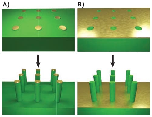
Nanowires can then be produced by etching the extraneous material from the wafer. Depending on the process, the resist may be used directly as the etch mask or may serve as the template for deposition of a more stable mask material, such as gold. Wet chemical etchants, like potassium hydroxide (306568), or an electrochemical etchant can then be used to etch the pattern, as illustrated in Figure 1A. This technique often produces tapered rather than cylindrical wires due to etching underneath the mask. This problem can be minimized by the use of anisotropic etchants, but it is rarely completely eliminated.4 One approach to achieving cylindrical vertical wires is to replace the wet chemical etch with a highly anisotropic deep reactive ion etch (DRIE), which can achieve vertical nanowires that are tens of microns in length. Alternatively, the pattern can be inverted and metal-assisted etching used,5 illustrated in Figure 1B, to achieve similar anisotropic structures.
Alternate approaches to conventional lithography promise higher resolution than can be achieved with optical lithography and higher throughput than is possible with conventional methods. Nanosphere lithography (NSL), for instance, involves the selfassembly of a monolayer of polystyrene nanospheres onto a substrate in a close-packed lattice.6 These spheres serve as a mask for the deposition of a metal or other masking material and are subsequently removed after deposition. Nanoscale patterns also can be produced through mechanical transfer with nano-imprint lithography (NIL).7 A high resolution master pattern is produced with a cost-intensive technique such as electronbeam lithography. This master is then pressed into the resist material to transfer the pattern.

Figure 1.Top-down fabrication methods. A) Lithographic patterning of a metallic mask followed by anisotropic etching, such as DRIE. B) Lithographic patterning of exposed regions followed by anisotropic metal-assisted chemical etching.
Benefits and Issues
Top-down nanowire fabrication is enticing due to the ease with which ordered arrays of nanowires can be constructed. This facilitates electrical contact to the nanowires and their integration into large-scale devices. Additionally, many of these processes are compatible with standard microelectronics industry processes, enabling their scale up.
Top-down fabrication does present several drawbacks. The applicability of photolithography to these processes diminishes as the desired length scales decrease, requiring the implementation of more advanced methods such as extreme ultraviolet (EUV) lithography. Alternatives to photolithography, like electron-beam and scanning probe lithographies, are direct-write techniques, requiring slow serial writing of individual elements. Parallelization of these techniques will be necessary for industrial-scale production. Nanowires formed by top-down processes also frequently lack complex electronic characteristics. When etched from a wafer, any desired modulation of composition must be encoded into the wafer by techniques like molecular beam epitaxy (MBE) or encoded after growth through implantation methods. This processing can greatly increase the material cost of nanowire devices compared to bottom up techniques.
Bottom-Up Synthesis
In contrast to top-down techniques, bottom-up processes are derived from a chemist’s toolkit, where molecules are assembled piece-by-piece and scaled up to produce materials thousands of times larger than the average molecule. Bottom-up syntheses are additive, like the growth of a tree from a small seed, using chemistry to control structure.
Vapor Phase
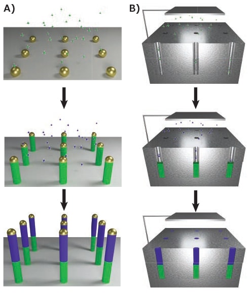
The anisotropic growth of nanowires is frequently accomplished using nanoparticle catalysts and gas-phase precursors. One of the most common methods is vapor-liquid-solid (VLS) growth, wherein gaseous precursors of the desired nanowire material, such as SiCl4 (215120) for silicon, dissolve into a liquid-metal catalyst.8 As the catalyst becomes supersaturated, the solid nanowire crystallizes from the liquid catalyst, as illustrated in Figure 2A. This synthesis involves a chemical vapor deposition (CVD) system, in which the temperature, pressure, and flow rates of precursors can be regulated. The conditions must be controlled to minimize non-catalytic growth of material on the side of the nanowire, which would disrupt the cylindrical geometry. Noble metal nanoparticles commonly serve as the initial seed for nanowire growth. For the VLS process, the metal must form a liquid droplet that serves as the catalyst. In many cases, this droplet forms a eutectic composition that melts at a lower temperature than the pure metal or semiconductor material. However, when synthesizing binary or ternary materials that contain a low melting metal, such as Ga in GaAs, the VLS process can be self-catalyzed using a Ga liquid droplet that is continuously supplied by a vapor-phase precursor such as trimethylgallium (730734).

Figure 2.Bottom-up synthesis methods. A) Vapor-phase growth of segmented nanowires through the VLS process, with modulation of the gaseous precursor resulting in controlled compositional changes. B) Solution-phase growth of nanowires through electrochemical deposition into anodic aluminum oxide (AAO). A similar segmentation process is possible.
VLS processes are advantageous because they allow for compositional control. Dopant materials, such as phosphine for silicon, can be introduced and removed repeatedly throughout the nanowire growth, producing superlattice structures with modulated electronic properties.9 Similarly, changing the ratio of the components in a ternary structure, like GaAsxP1–x, can produce nanometer-scale bandgap modulation10 and quantumwell structures.
Although metal catalysts are commonly dispersed on a solid substrate, a variant called aerotaxy utilizes catalysts suspended in the reactor to achieve high growth rates.11 A lower temperature process, called vapor-solid-solid (VSS) growth, uses many of the same principles as VLS growth.12 However, the catalysts are solid rather than liquid, altering the kinetic processes. Rather than dissolving and supersaturating in a liquid, the precursors diffuse through the interface between the catalyst and nanowire in order to add material. This slows down the growth process, allowing for more abrupt (to the atomic level) compositional changes in the nanowire.
Contamination of the catalyst material in the nanowire can be disadvantageous for certain processes, so non-catalyzed syntheses have also been developed. Templated growth provides one pathway to achieve the anisotropy needed for nanowires. AAO, produced by electrochemical etching, contains a honeycomb of nanometer-scale channels, offering the geometry required for producing arrays of vertical nanowires. Conventional vapor deposition techniques (CVD, sputtering, etc.) can be used to fill these channels, producing nanowires when the template is removed. A patterned substrate can be used for selectivearea epitaxy (SAE), in which epitaxial growth occurs in exposed regions, but deposition onto the mask material does not occur.13 The presence of screw dislocations has also been demonstrated as a mechanism to induce catalyst-free nanowire growth.14
Solution Phase
Many of the techniques employed in the vapor phase have analogies in the liquid phase. The solution-liquid-solid (SLS) mechanism is similar to that of VLS, except nanowire precursors are dissolved into a high-boiling liquid, such as squalane (234311), and the catalysts are suspended therein.15 AAO substrates can also be used for templated solution growth, using electrochemical deposition to fill the channels16 as shown in Figure 2B. Drawing upon the solution-phase synthesis of nanoparticles, redox reactions can also be used to produce nanowires.17 Seed particles are first grown by a rapid reduction of a dissolved precursor with a strong reducing agent like sodium borohydride. Secondary growth is achieved with a weaker reducing agent, like l-ascorbic acid, to prevent additional seed particle production. The nanowire anisotropy is achieved by controlling surface chemistry. The introduction of surfactants that selectively alter the surface energy of particular crystal facets, such as hexadecyltrimethylammonium bromide (CTAB, 52370), directs growth along particular axes, producing nanowires.
Benefits and Issues
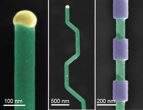
Bottom-up synthesis provides the opportunity for explicit control of nanowire composition during growth, enabling the production of complex superlattice structures. This compositional control can be used to encode novel electronic properties such as quantum well photodiodes, as well as provide a template for subsequent processing. Selective etching of these superlattice structures has been shown to produce a wide variety of shapes and structures that can be used in photonics, electronics, and memory18 (Figure 3).
The main challenge facing further development of technologies based on bottom-up nanowires involves their integration into large-scale devices. Wires grown in vertical arrays can be used in a similar fashion to those fabricated by top-down methods, but many growth processes instead produce disordered “forests” of nanowires or solutions of nanowires. Recent research efforts have focused on how to assemble and organize the nanowires so they can be interfaced with conventional manufacturing steps. The incorporation of these techniques will prove essential to moving nanowires from the laboratory to the factory.

Figure 3.Nanowire structures. A) False-color SEM of a silicon nanowire grown by VLS (green) and the metal catalyst at the tip (yellow). B) Falsecolor SEM of crystallographic kinking that can be accomplished by manipulating the reaction conditions. C) False-color SEM of morphology that can be achieved by modulating the composition during growth, followed by etching.
Conclusions
Nanowires possess a number of unique properties derived from their highly anisotropic but often single-crystalline structure. They are highly sensitive to changes in surface chemistry due to their high surface area. They also provide for highly anisotropic charge transport, allowing for rapid radial transport or charge injection combined with long conduction pathways along the nanowire axis. The diameter of nanowires is sufficiently small to allow many bulk properties to be manipulated by the nanowire geometry. Nanowire optical properties can be tuned by manipulating the diameter, which changes the optical resonant modes that can be supported by the nanowire. Similarly, thermal transport can be altered through nanoscale geometry. Due to their small radii, nanowires can relieve strain more efficiently than bulk materials, making them much more flexible.
The primary concern that underlies nanowire synthesis or fabrication is how to achieve the necessary anisotropy. Top-down fabrication techniques utilize bulk crystals and use patterning to selectively remove material to produce nanowires. Conversely, bottom-up techniques grow the nanowires from reactive precursors, using nanoparticles or nanostructured templates to provide the anisotropy. The complementary integration of topdown and bottom-up techniques will be vital to the integration of nanowires with industrial processes. Nanowires present an opportunity to overcome bulk material limitations through nanoscale electronic and structural control, which will enable a new generation of devices and applications.
Materials
References
To continue reading please sign in or create an account.
Don't Have An Account?