Organic & Hybrid Electronics for Optical Analysis
Introduction
Organic semiconductor materials and devices, such as organic light emitting diodes (OLEDs), organic solar cells (OSCs), and organic photodetectors (OPDs), continue to attract considerable interest. Their use has expanded into novel applications including photoluminescence (PL)-based (bio)chemical sensors, spectrometers-on-a-chip using OLED pixels as excitation sources and OPDs for signal monitoring,, and sensitive medical devices.
Commercial viability of any sensing platform increases when all of its components can be easily integrated into a compact, field-deployable device, and is enhanced even more when the fabrication is simple, scalable, and low-cost. Traditional light sources such as lasers or LEDs cannot be easily integrated with other components due to geometrical, operational, or size constraints. One promising approach, however, is a sensing platform based on an OLED excitation source (or an array of OLED pixels), a luminescent sensing thin film, and a PL-monitoring OPD. The organic components can be easily fabricated on flexible plastic substrates, enabling development of wearable sensors and other devices. Further, while the lack of long-term stability remains a concern for OLED-based devices, many sensors are expected to be deployed in short-term or disposable situations. Traditional photodetectors (PDs) include charge coupled device arrays, photomultiplier tubes (PMTs), and inorganic photodiodes, which also hamper integrability. With their potential for miniaturization, all-organic sensors eliminate issues related to portability and deployability, simplify fabrication, and reduce cost. The ability to fabricate simplified and integrated sensors reduces the need for trained operators, while maintaining high sensitivity, with potential for use in many diverse applications. When fabricated in a small-size array, allorganic sensors can be used for monitoring multiple analytes, either by addressing a single OLED pixel individually or by simultaneously addressing groups of pixels. Recently, the use of hybrid perovskite-based PDs (PPDs) in sensing applications has gained attention due to their fast response and high responsivity.
In this article, we summarize some of the developments in the area of organic and hybrid electronics in optical analytical applications, including biochemical sensors and the spectrometer-on-a-chip platform.2,3 Here, we will discuss sensing examples based on monitoring oxygen. PL-based O2 sensors have been studied extensively,1 and gas-phase and dissolved oxygen (DO) monitors based on them are available commercially. The development of reliable, sensitive, and compact field deployable sensors and devices for medical, biological, and water treatment applications continues. PL-based sensors are preferred for their high sensitivity, low maintenance requirements, and infrequent need for calibration. Typically an oxygen-sensitive dye (e.g., Pt or Pd octaethylporphyrin (PtOEP (Cat. No. 673625) or PdOEP), respectively) is embedded in a thin polymeric (e.g., polystyrene (PS)) or sol-gel film that is structurally integrated with the excitation source and the PD. When oxygen molecules collide with photoexcited dye molecules, their PL is quenched with a dose-dependent decrease in the PL intensity I and decay time T. Calibration lines and thus the oxygen level can be obtained (ideally for a dynamic quenching process) using the Stern-Volmer (SV) equation:
(1) I0/I = T0/T = 1 + KSV[O2]
where I0 and T0 are the unquenched values, and KSV is the film and temperature dependent SV constant. The sensitivity S is defined as
(2) S Ξ I0/I(100% O2) = T0/T(100% O2)
Pulsing the OLED allows monitoring of the O2 via the intrinsic attribute t. This approach is valid provided that t is much longer than both the OLED’s electroluminescence (EL) decay time and the PD’s response time. Monitoring t eliminates the problem of stray or background light stemming from the typically broad EL spectrum, whose long-wavelength tail often extends into the PL band of the sensing element. Additionally, when operating in the t mode, moderate changes in the intensity of the excitation source and changes in the sensing component, such as dye leaching, have minimal effect on the sensor’s response. As a result, the need for frequent calibration and optical filters (needed in the I detection mode for EL long wavelength-tail blocking) is eliminated, resulting in a more compact and reliable device.
Sensitive monitoring of other (bio)chemical analytes such as glucose, lactate, cholesterol, and ethanol is often based on oxygen consumption during oxidation of the analytes that is catalyzed by their specific oxidase enzyme. For example, glucose is oxidized in the presence of glucose oxidase (GOx) and O2 to yield gluconic acid with the oxygen reduced to H2O2 . Lactate oxidase (LOx) and alcohol oxidase (AOx) similarly catalyze the oxidation of lactate and ethanol, respectively. In sealed containers, where there is no DO other than the initial concentration, the change in [DO] is equal to the initial analyte concentration ([analyte]initial) if the initial DO concentration is more than the initial analyte concentration. As the analyte is completely converted into product, the final DO concentration is given by
(3) [DO]final = [DO]initial − [analyte]initial
And the SV equation becomes:
(4) I0/I = T0/T = 1 + KSV × {[DO]initial − [analyte]initial
Where I is intensity, and T is the lifetime. Thus, a plot of 1/t vs. [analyte]initial, to generate calibration lines, will ideally be linear up to the point where the initial DO concentration is equal to the initial analyte concentration.
The OLED-based sensing platform was also utilized for monitoring relative humidity, pH, hydrazine, and anthrax lethal factor.1,8
Toward All-organic O2 Sensors
OLED/Sensing Film Integration
Figure 1A shows the original design of an OLED-based oxygen sensor with an inorganic PD in a back-detection geometry, where the OLED and the PD are on the same side of the sensing film; the OLED and the sensing film are on opposite sides of a common transparent substrate.1 The disadvantage of this design is that the PL is partially blocked by the nontransparent OLED cathode. Figure 1B shows the use of a microcavity (µC) OLED rather than a standard bottom emitting OLED, where the OLED stack is deposited between a transparent anode such as indium tin oxide (ITO) (Cat. Nos. 703192, 576360 and 578274) and a metal cathode.8 In µC OLEDs, the transparent anode is replaced by a very thin semi-transparent metal to form an optical cavity, with a proper design and tuned layers’ thickness so it can be tailored to emit at a particular wavelength with a significantly narrowed full width at half maximum (FWHM). The sharper µC OLED EL bands minimize overlap and hence minimize interference with the PL of the sensing probe.
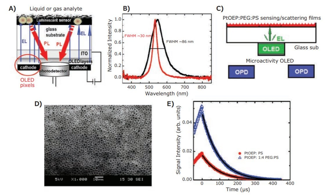
Figure 1.Toward all-organic optical (bio)chemical sensors. A) The initial design with two-component integration of OLED/sensing film in back-detection geometry. Reproduced with permission from reference 1, copyright 2008 IOP Publishing Ltd B) EL spectrum of standard and µC green OLEDs. C) Replacing standard OLEDs with µC OLEDs and the inorganic PD with OPDs + using an enhancing PEG-doped PS sensing film. Reproduced with permission from reference 8, copyright 2013 Elsevier B.V. D) SEM image of the microporous PL-enhancing sensing film. Reproduced with permission from reference 9, copyright 2011 OSA. E) PL intensity (measured with a PMT) vs time in a N2 atmosphere using pulsed OLEDs, showing the increased PL signal with the PtOEP:PEG:PS sensing probe; the black lines are the exponential fits for extracting T. Reproduced with permission from reference 8, copyright 2013 Elsevier B.V.
In Figure 1C, the sensing film is PtOEP:PEG:PS, where PEG is polyethylene glycol (Cat. Nos. 1546580, 1546445 and 1546569). The film is prepared by drop-casting a toluene solution of PtOEP:PEG:PS at specific mixing ratios. The high molecular-weight PS with glass-matching refractive index n ~1.55–1.59 has a lower solubility in toluene than the low molecular weight PEG. Hence, during the drying process PS precipitates first, while small PEG-rich droplets form on the film’s surface and in the bulk film. During evaporation the PEG droplets shrink, leaving behind surface and bulk PEG-coated PS micropores, as shown in the SEM image (Figure 1D) of a film with PEG:PS ratio of 1:4.9 The film resulting from this process enhanced the PL signals 2.7 fold compared to PtOEP in a PS matrix without PEG, as shown in Figure 1E. Using the PtOEP:PEG:PS sensing improved sensitivity from S ~11 to S ~21. Results for OPD replacing inorganic more bulky PDs are described later.
Figure 2 illustrates detection of multiple analytes in solution following an OLED excitation pulse using two different designs of integrated sensors.10 Figure 2A shows the sensor array in operation, where analysis is performed consecutively using a single inorganic PD.
Also shown in Figure 2A are the PL decay curves and decay times for oxygen, glucose, ethanol, and lactate. Pixel pairs 1 and 6 show the green EL of bare OLEDs. Pixel pairs 2–5 show the pixels’ response to the analytes. The orange color results from the mixture of green EL background and red PL of the PtOEP:PS sensing film. In the other design (Figures 2B and 2C) the analytes’ detection is simultaneous with the solutions in sealed containers. This design is more compact (Figure 2B), with the sensing films on glass serving as the bottom of the containers. Each container contains an analyte or a mixed solution of the analyte and a specific enzyme that catalyzes its oxidation. The OLED pixels are individually addressable, and can operate simultaneously as well. The pixels are defined by the overlap between the mutually perpendicular ITO and Al electrode stripes. The pixel size is typically 2 × 2 mm2, though 0.3 × 0.3 mm2 pixels have also been tested and found similarly adequate for use as the excitation source. There was no crosstalk between the OLED pixels, and two pixels were used for each of the four analytes. Figure 2C shows calibration lines of 1/t vs glucose or lactate concentration, and analysis results for solutions with analyte mixtures. As expected, the lines follow Eq. (4) perfectly. These latter results point to a lower limit of detection (LOD) of ~0.02 mM analyte.
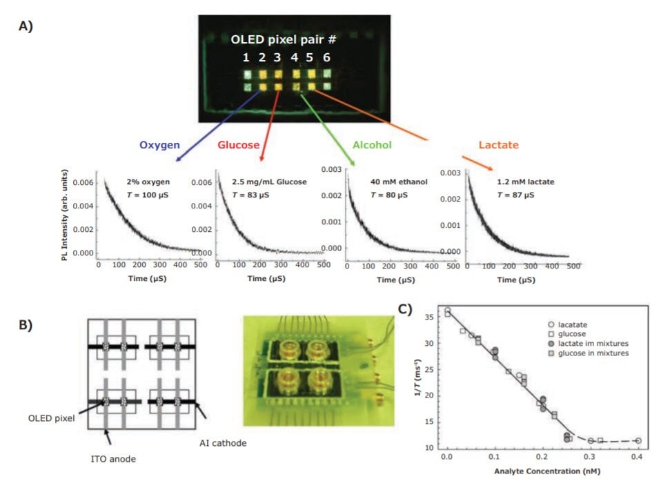
Figure 2.PL-based multianalyte detection of oxygen, glucose, ethanol, and lactate, using a structurally integrated OLED-based platform. A) Multipixel excitation platform with a single PD. B) Schematic and image of the multianalyte sensor array with 4 Si photodiodes. The four sample holders contain (i) no enzyme, (ii) glucose oxidase, (iii) ethanol oxidase, and (iv) lactate oxidase. C) 1/t vs the initial glucose or lactate concentrations, separately (open symbols) and in mixtures (grey symbols); the sensing films are at the bottom of sealed containers. Reprinted with permission from reference 10, copyright 2008 Elsevier B.V.
In a similar approach, the viability of an OLED-based sensing platform was demonstrated for a lab-on-CD.11 This platform is promising for commercial applications, due to its simple control of fluid flow via CD rotation, suitability for various samples at a wide range of flow rates, compactness, and versatility of functions.12-15 In addition, since the lab-on-CD is fabricated on plastic substrates it is low cost, disposable, recyclable, feasible for high-volume manufacturing, and biocompatible. Furthermore, the thin OLEDs can be easily integrated with the CD, and are also compatible with microfluidic architectures.
Microfluidic features were generated by ultrasonic microembossing on foamed polypropylene (PP) CDs. The embossed features functioned as reservoirs, channels, valves, and reaction chambers (Figure 3A). A compatible array of two mm thick surface mounted Si based photodiodes as PDs was designed. The combination of the OLED/PD arrays and the microfluidic structures enabled simultaneous monitoring of glucose, lactate, ethanol, and DO in four separate CD segments using a standard CD player compatible with a PC. The concentration of the analytes was determined following CD rotation for reagent mixing and flow direction. In one monitoring approach, ~200 µL of known analyte concentrations were loaded into the reaction chamber (RC) and ~30 µL of the appropriate enzyme solution was loaded into an enzyme chamber in the bio-CD. Following CD rotation, the appropriate valve (i.e., an enlarged section in the microfluidic channel) “bursts”, and the enzyme solution is directed into the sealed RC (total volume 230 µL). Calibration curves for each of the analytes were generated and concentrations in mixtures were determined for each segment of the bio-CD. Figure 3 shows also images of the CD-OLED-PD sensing platform.

Figure 3. A) General structure of microfluidic features on lab-on-CD and B) Images of the CD-OLED/PD sensing platform: left—the preamplifier board with the four Si photodiodes; middle—the PD array and the green OLED pixels in operation; and right—the complete device with the sensor films (pink) on the polypropylene CD; the lit OLED pixels are also visible. The sensing films form the bottom of the reaction chambers with the OLEDs underneath. Reprinted with permission from reference 11, copyright 2010 The Royal Society of Chemistry.
OLED/Sensin /Thin-film PD Integration
Following integration of the OLED and the sensing film, a thin film PD was added. Inorganic PDs based on hydrogenated amorphous Si and better, nano-crystalline Si can be used, but only for monitoring intensity.16 The response time of such PDs is longer than the PL decay times due to charge recombination and trapping in defects, but OPDs and PPDs are more promising.
A bulk-heterojunction (BHJ) OPD based on poly(3- hexylthiophene) (Cat. Nos. 900549, 900563 and 900550) and phenyl-C61-butyric acid methyl ester (Cat. Nos. 684457, 684457 and 684430) (P3HT:PC61BM) was engineered to optimize sensitivity to the red emission of the sensing film. A fast response time enabled the monitoring of analytes in both I and t detection modes.17 Figure 4 shows the PL decay curves and the SV calibration curves using green emitting LEDs or OLEDs. The PtOEP was embedded in a TiO2 nanoparticle (Cat. Nos. 791547, 791555 and 798495) doped PS matrix. TiO2 nanoparticles improve the EL and hence PtOEP’s absorption by photon scattering within the PS matrix, increasing the optical path.18 When monitoring the analytes via T, the excitation sources were operated in a pulsed mode with 100 µs pulse width at 50 Hz.
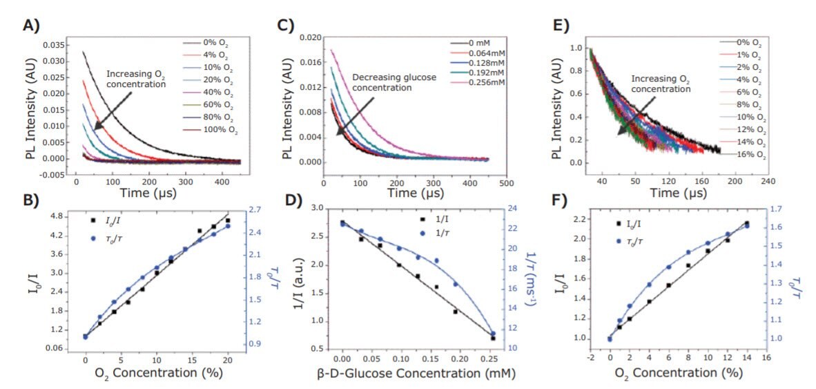
Figure 4.The effect of concentration of gas-phase O2 A) and glucose C) on the P3HT:PCBM OPD’s temporal photocurrent response. Excitation source was an LED. B) and D) are I- and T -based SV calibration curves corresponding to A) and C), respectively. For OLED excited O2 sensor, E) and F) show the effect of O2 concentration on the OPD’s temporal response and the corresponding SV calibration curves, respectively. Reprinted with permission from reference 17, copyright 2010 WILEY-VCH Verlag GmbH & Co. KGaA, Weinheim.
As shown, the dynamic range and sensitivity of these first generation all-organic sensors were limited and the signals were sometimes noisy. Nonetheless, the results demonstrated initial feasibility of the all-organic sensing paradigm. Subsequent developments significantly increased sensitivity and concentration range (shown next).8 In particular, the use of a PPD, currently under development, is promising for sensitive detection in the time domain.
In the previous example (Figure 4), a polymeric P3HT:PC61BMbased OPD was used. Figure 5A shows the external quantum efficiency (EQE) spectrum of such an OPD together with the EQE spectrum of an organic small molecule-based CuPc/C70 OPD (CuPc is copper(II) phthalocyanine, Cat. Nos. 702854, 546682 and 546674).8 Also shown is the EL spectrum of the green-emitting OLED and the red PL of PtOEP. As seen, the polymeric OPD is very sensitive to the green EL and less so to the red PL. While the EQE of the CuPc/C70-based OPD is generally lower, it presents better sensitivity to PtOEP’s PL and lower sensitivity to the OLED’s EL.
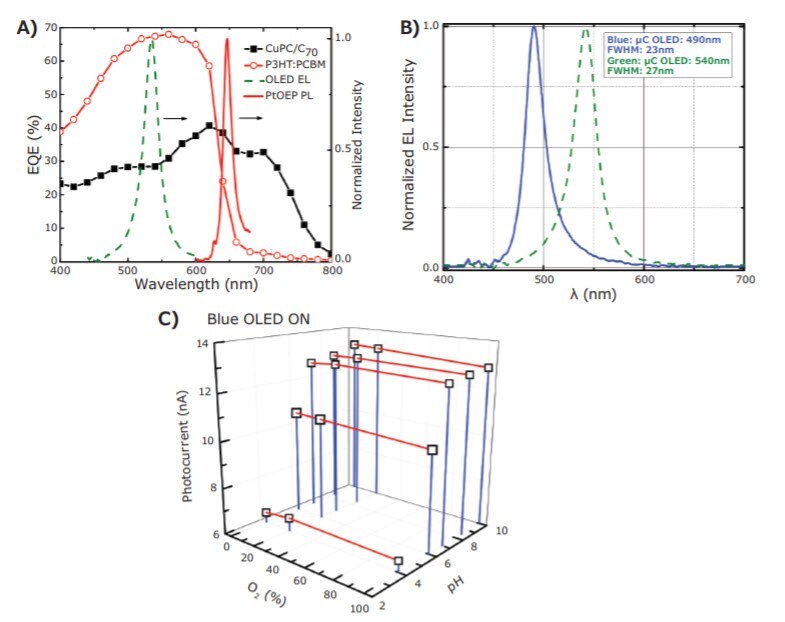
Figure 5. A). EQEs of CuPc/C70 and P3HT:PCBM based OPDs. The device structures are ITO/1 nm LiF/15 nm CuPc/30 nm C70/3.5 nm BPhen/120 nm Al and ITO/PEDOT:PSS/P3HT:PCBM/ Ca/Al. Also shown are the EL of the green µC OLED (green dashed line) and red PL of the PtOEP:PEG:PS sensing film (red line). B) The EL of the green and blue µC OLEDs. C) The signal intensity detected by the P3HT:PCBM OPD at different O2 and pH levels with the blue µC OLED. Reprinted with permission from reference 8, copyright 2013 Elsevier B.V.
Using these two OPDs, an all-organic sensing platform for simultaneously monitoring DO and pH was constructed.8 Multiple methods to improve the sensor’s performance and the data analysis were utilized. Two µC OLEDs, green and blue emitting (Figure 5B), were fabricated combinatorially with the normal direction peak EL wavelengths designed for the O2 -sensitive PtOEP and pH-sensitive fluorescein, respectively. In this way, 2D data for monitoring these two analytes could be extracted. Furthermore, from the transient decay signals following an OLED pulse, the PL bands related to the DO and pH could be resolved by employing both the T and I detection modes, respectively. Hence, the two analytes could be monitored simultaneously: the DO with the green µC OLED + the CuPc/C70 OPD in the T mode; and the pH with the blue µC OLED + the P3HT:PCBM OPD in the I mode. Another feasible OPD is based on PTB7:PCBM (PTB7 is poly({4,8-bis[(2-ethylhexyl)oxy]benzo[1,2-b:4,5-b′]dithiophene2,6-diyl}{3-fluoro-2-[(2-ethylhexyl)carbonyl] thieno[3,4-b] thiophenediyl}), Cat. No. 772410).3 This OPD is excellent when used in conjunction with a near UV µC OLED based on CBP (4,4′-bis(N-carbazolyl)-1,1′-biphenyl, Cat. Nos. 699195 and 660124).3 The EL of the CBP µC OLED peaks at ~385 nm, where the PtOEP strongly absorbs. However, it operated successfully only in the I mode.
Another example of an all-organic monolithically integrated OLED/OPD sensor was also demonstrated. Other OPDs, which can be utilized in all-organic optical sensors, are being investigated. One example is the synthesis of solution-processed PIDT-TPD (poly[4,4,9,9-tetrakis(4-hexylphenyl)-4,9-dihydro-sindaceno[1,2b:5,6-b′]dithiophene-2,7-diyl-alt-5-(2-ethylhexyl)-4Hthieno[3,4-c]pyrrole-4,6(5H)-dione-1,3-diyl]), which has several attributes that make a good OPD, including a maximal 52% EQE at 610 nm, 1 nA/cm2 dark current, and a high detectivity of 1.44 x 10¹³ Jones under -5 V bias.
A narrow-band (FWHM <30 nm) photomultiplication-type OPD utilizing P3HT:PC61BM was also described. Improvement was reported in a planar heterojunction structure with the PC61BM layer positioned next to the Al cathode, allowing for a thin film (150 nm) OPD with a high detectivity under a bias of -5 V.
Hybrid Perovskite-Based PDs
While OPDs show promise as flexible devices, further improvement of their performance is hindered by their low charge mobility and long response time. In contrast, PPDs exhibit high charge mobility, EQE, sensitivity, and fast response times. Indeed, the potential of hybrid PPDs has been demonstrated in various applications. For example, a PPD with a sub-ns response time, which is promising for imagers in digital cameras, was used for measuring the PL lifetimes of organic and hybrid materials. These measurements provide insight on the material’s quality, since the PL decay time is affected by defects and dopants.
Development of PPDs continues. For example, perovskite photomultipliers with high gain have been fabricated by trapand interface-engineering using a perovskite rich in PbI2 . Tunable, narrow band (e.g., EQE FWHM ~28 nm) PPDs were fabricated using two perovskite layers where the first layer filters light and the second is the active layer. The sensitivity and wavelength of PPDs can be tuned by changing the bromide:iodine ratio in CH3NH3PbBr3-xIx in both layers. Such PPDs do not require a bandpass filter and their lowest reported time constant was ~100 ns, with the possibility for improvement. This type of PPD is a promising approach for designing an array for monitoring multiple analytes with different, specific wavelength sensing probe emissions.
The high responsivity and fast response time of PPDs has produced promisig initial results for O2 sensing. Figure 6 shows the EQE spectrum of a PPD with the structure ITO/PTAA/ perovskite/C60/BCP/Cu where PTAA is poly(triaryl amine) (Cat. No. 702471) and BCP is bathocuproine (Cat. Nos. 699152 and 140910).26 As seen in Figure 6, the high EQE is maintained across the broad wavelength range from ~375 to ~750 nm. The ~8 mm2 response time of PPDs was ~300 ns (increases with the PPD’s active area), which is ~10 times faster than the PL decay time of O2 -based (bio)chemical sensors exposed to 100% gas-phase level. As such, the PPD is suitable for monitoring O2 via the advantageous T measurements (Figure 6B). Optimization of both the PPD and the optical sensor set up are ongoing, though even at this early stage the performance exceeds that of some OPDs, in particular when measuring t (Figure 4), with S ~16.
For comparison, Figure 6 shows another set of results using allorganic O2 sensors. Figure 6C shows the EQE spectrum of the viable PTB7: PCBM-based OPD.3 This OPD is excellent when used in conjunction with a near UV µC OLED based on CBP.3 The EL of the CBP µC OLED peaks at ~385 nm, where the PtOEP strongly absorbs and S ~27 (Figure 6D); however, so far it operates successfully only in the I measurement mode.
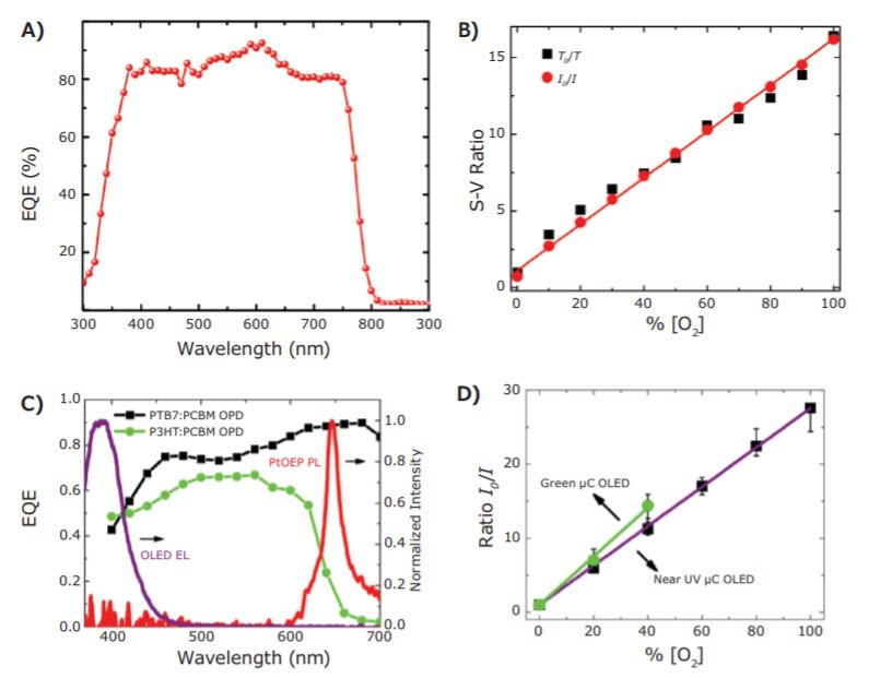
Figure 6. A) The EQE spectrum.29 B) Initial results showing SV plots as measured in both I and t modes, of an ITO/PTAA/perovskite/C60/BCP/Cu PPD. C) EQE spectra of P3HT:PCBM and PTB7:PCBM-based OPDs, and the normalized EL spectrum of the near-UV µC OLED (purple line) and PL spectrum of PtOEP embedded in 1:9 PEG:PS. D) The SV ratio I0/I for the green mC OLED/P3HT:PCBM OPD and near UV µC OLED/PTB7:PCBM OPD. Reprinted with permission from reference 8, copyright 2013 Elsevier B.V.
OLED/OPD Based Spectrometer on a Chip
While OLEDs have been widely studied for applications in displays and solid-state lighting, multicolor (MC) OLEDs are of interest not only for simple fabrication of display or lighting subpixels, but also for their use in miniaturized analytical devices. OLEDs with multiple-wavelength emission on simple substrates can operate as a compact spectrometer or form individually addressable, excitation-source pixels for bio(chemical) sensing of different analytes.1 However, conventional OLEDs generally have broad emission spectra. With the growing industrial requirements for compact, potentially disposable analytical devices, a simpler, more economical method to fabricate narrow-band MC µC OLEDs is highly desirable.
In this section we provide two examples of such MC µC OLED arrays, which, when combined, cover the 370–693 nm spectral range. The approach is based on combinatorial fabrication of MC µC OLEDs, where the precise value of the peak emission wavelength λem,max is controlled by the optical cavity length l μC, , and lμC is controlled by the thickness of a “spacer” layer fabricated between the metal electrodes of the OLED, which also serve as the µC mirrors. The second example (which expanded the spectral range down to 370 nm) demonstrates additional integration of OPDs with the MC µC OLED array, and provides guidance in designing OPDs for optimal sensitivity and performance.
In the first example,2 covering the 493–693 nm band, a layer of MoOx was used as the spacer. Sub-stoichiometric MoOx (x <3) (Cat. No. 900151) is widely used as a hole injection layer (HIL) due to its ease of processing, high conductivity, and favorable energy alignment. As shown by Liu et al.,2 it is also a good injection and spacer material for tuning the optical length of µC OLEDs, while maintaining favorable current density-voltage (J-V) behavior. Additionally, it is found that MC µC OLEDs with this heat-resistant HIL are more stable at high voltages, with enhanced maximum normal direction EL. This is beneficial for sensitive sensors, which may require intense excitation.
To demonstrate the potential of the OLED-based spectrometeron-a-chip, Liu et al.,2 fabricated 2D combinatorial arrays of blue-to-red ~1.5 mm diameter µC OLED pixels on a 2 in. x 2 in. glass/ITO substrate by thermal evaporation (Figure 7A). The 2D MC µC OLEDs were obtained by simply changing the Alq3 layer thickness during combinatorial fabrication. The structure of the 12 pixels was:
40 nm Ag/x nm MoO3 /49 nm α-NPB/1 nm 8 wt%
Ir(MDQ)2(acac):α-NPB/y nm Alq3 /1 nm LiF/~100 nm Al
where α-NPB is N,N′-di(1-naphthyl)-N,N′-diphenyl-(1,1′-biphenyl)- 4,4′-diamine (Cat. Nos. 556696 and 734594), Ir(MDQ)2(acac) is iridium (III) bis(2-methyldibenzo [f,h] quinoxaline) (acetylacetonate) (Cat. Nos. 901074 and L512206), Alq3 is tris(8-hydroxyquinoline) Al III (Cat. Nos. 444561 and 416282), x = 2, 5, 10, 15, 20, or 35 nm, and y = 56 (Devices A) or 64 nm (Devices B).
The Ir(MDQ)2(acac)-doped layer was responsible for the red emission peaking at ~610 nm and Alq3 for the green emission peaking at ~525 nm. As x varied from 2 to 35 nm, with y fixed at 56 nm, the peak emission shifted from 493 nm sky blue (Device A-D1) to 639 nm red (Device A-D6) due to the μC (Purcell) effect. When y was increased to 64 nm, the longest wavelength increased to 650 nm (Device B-D6), and additional wavelengths were added in the 493–650 nm range. Note that the narrowest FWHM was ~22 nm for device A-D1 and it broadened for thicker MoOx layers. Importantly, at a given voltage all OLEDs’ brightness and efficiencies were comparable.
A spin-coated P3HT film was used to demonstrate the spectrometer (Figure 7B). For each pixel, a background signal was obtained by shining the OLED directly onto the PMT, while the actual signal was collected after the light passed through the P3HT film. The ratio of the difference of the two signals to the background is related to the P3HT film absorption. As seen from the individual data points in Figure 7B, the resultant absorption spectrum agrees with the reference spectrum.
In the second example, combinatorial arrays of efficient, near UV/deep-blue OLEDs were fabricated, and used to demonstrate the feasibility of the spectrometer-on-a-chip down to 370 nm.3 Arrays with pixels emitting at different wavelengths in this range are of strong interest for analytical applications. In addition, these OLED arrays were combined with OPDs based on P3HT:PCBM or the more sensitive PTB7:PCBM, demonstrating an all-organic spectrometer-on-a-chip.
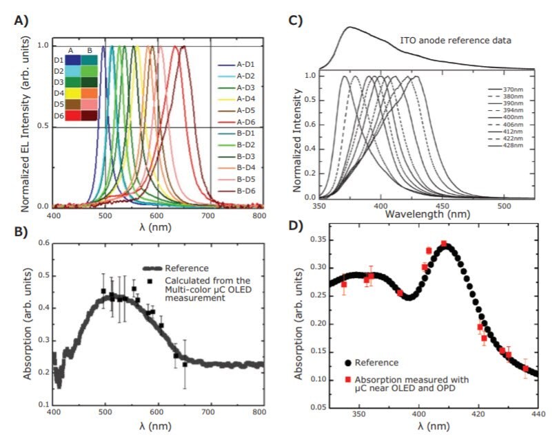
Figure 7.Spectrometer-on-a-chip. A) EL spectra of combinatorial array of 40 nm Ag/x nm MoO3 /49 nm α-NPB/1 nm 8 wt% Ir(MDQ)2(acac):α-NPB/y nm Alq3 /1 nm LiF/~100 nm Al OLEDs. B) Absorption spectra of P3HT as measured by the array shown in (A) and by a reference spectrophotometer. Reprinted with permission from reference 2, copyright 2011 American Institute of Physics. C) EL spectra of near UV-deep blue combinatorial 15 nm Al/5 nm MoOx/20 nm TAPC/x nm CBP/y nm BPhen/1 nm LiF/~100 nm Al OLED array vs the EL spectrum of a reference device with an ITO electrode and D) absorption spectra of an Alexa Fluor 405 film using a reference and the integrated OLED/OPD arrays. Reprinted with permission from reference 3, copyright 2015 WILEY-VCH Verlag GmbH & Co. KGaA, Weinheim
The structure of the OLED pixels comprising the arrays was
15 nm Al/5 nm MoOx/20 nm TAPC/x nm CBP/y nm BPhen/1 nm LiF/~100 nm Al
where 15 ≤ x ≤ 30 nm and 25 ≤ y ≤ 40 nm.
Figure 7C shows the EL spectra of the different OLED pixels in the near UV/deep blue array. As clearly seen, λem,max increases from 370 nm to 430 nm as x and y increase. As in the case of the sky blue-to-red array above, the FWHM increases with λem,max. Figure 7D shows the absorption spectrum of an Alexa Fluor 405 film using this OLED array.3 As clearly seen, the data points obtained with the OLED/OPD arrays are in excellent agreement with the reference spectrum.
Medical Applications
Organic optoelectronic sensors have also found use in medical applications.4,5 Figure 8A shows an example of green and red printed polymer LEDs (PLEDs) that were used as light sources in reflection-mode pulse oximetry, together with a silicon photodiode for measuring blood oxygenation on the wrist.5 The device measures arterial oxygen saturation and heart rate.
In another report, a flexible (bending radius of ~100 µm) ultrathin (3 µm) reflective pulse oximeter and photoplethysmograph (PPG) device was fabricated using OPD and PLEDs, including utilization of an on-skin digital display. In a more recent example, a skin-conformal, near-IR, ultrathin (3 µm thick) and ultra-flexible (bending radius of 3 µm) OPD was demonstrated. The device maintained operational stability when flexed over 103 cycles. Additionally, fingerprint-conformal PPG sensing with fast response was demonstrated. These attributes enable its use as a cardiovascular sensor.
A recent report describes a flexible PPG sensor composed of flexible red OLEDs and OPDs that are highly sensitive to red EL.34 The PPGs can be suitable for detection of various biological signals, and as an example of real-world application this flexible PPG was used to detect drowsiness, with performance similar to that of a conventional PPG sensor.
Other results have demonstrated the further potential of organic optoelectronic devices, which combine OLEDs and OPDs on flexible substrates, as low-cost, disposable, non-invasive optical sensors in medicine and sports. Figures 8B and 8C show an example of a wearable muscle contraction sensor.4 The application of this sensor, with a super yellow-based PLED that has a broad emission spectrum from 520 to 700 nm and a PTB7:PC70BM OPD, was demonstrated by showing that it could be used to control a robotic arm that mimicked the movement of a real arm. In the second example, a wearable flexible organic optoelectronic bandage was used for measuring tissue oxygenation, enabling long-term monitoring.

Figure 8. A) Schematics of a reflection-mode wrist pulse oximeter using green and red PLEDs as the light source together with a silicon PD. Reprinted with permission from reference 5, copyright 2017 John Wiley & Sons. B) Schematic principle of muscle contraction sensor showing an arm containing muscle fibers, and a probe bandage consisting of a light source and four photodiodes on top of the arm. C) Photograph of a thin flexible organic optoelectronic sensor. Reprinted with permission, copyright 2014 John Wiley & Sons.
Summary
The advantages of thin film-based devices, such as all-organic and hybrid optical, biological, and chemical sensors, are their small size (potential miniaturization), portability, and thus fielddeployability. Moreover, flexible all-organic devices can be adapted as wearable/badge-size monitors for diagnostic and therapeutic medical applications.
Further, organic and hybrid perovskite electronic devices hold promise for optical, analytical, and medical applications due to their ease of fabrication, unique simplicity of integration of various thin-film components, and potential low cost. OLEDs, which are promising as efficient light sources in luminescent sensor (micro) arrays for multiple analyte detection, can be easily integrated with thin-film sensing probes, and with thinfilm PDs, e.g., OPDs and potentially PPDs. Moreover, they are compatible with microfluidic architectures, and are often used in analytical applications.
OLEDs can be operated in a pulsed mode, which enables their use not only in the PL intensity I mode, but also in the PL decay-time t mode. This mode of operation eliminates the need for frequent sensor calibration and for optical filters. In improving the OLED sensing platform, standard bottom-emitting OLEDs were replaced by narrow-band µC OLED pixels, which are bright and efficient. Their narrower EL spectrum can be tailored to the absorption spectrum of sensing elements, significantly improving the sensor’s performance. Importantly, a MC µC OLED array, in conjunction with suitable OPDs, can serve as a spectrometer on a chip. As shown, PPDs, though not yet fully tested in conjunction with OLEDs, hold much promise because of their strong sensitivity and fast response time.
The utilization of compact, light-weight, and low cost thin-film organic and hybrid optical platforms for analytical applications is expected to increase dramatically as devices improve and these technologies are adopted in other applications. This platform technology is expected to help address ongoing security and safety issues, detect explosives, and monitor foodborne pathogens.
Acknowledgments
This work was supported in part by NSF grant ECCS 1608496. Ames Laboratory is operated by Iowa State University for the US Department of Energy (USDOE) under Contract No. DE-AC 02-07CH11358. The research was partially supported by Basic Energy Sciences, Division of Materials Science and Engineering, USDOE.
References
To continue reading please sign in or create an account.
Don't Have An Account?