产品名称
铟, foil, thickness 1.0 mm, 99.999% trace metals basis
InChI key
APFVFJFRJDLVQX-UHFFFAOYSA-N
InChI
1S/In
SMILES string
[In]
vapor pressure
<0.01 mmHg ( 25 °C)
assay
99.999% trace metals basis
form
foil
resistivity
8.37 μΩ-cm
thickness
1.0 mm
mp
156.6 °C (lit.)
density
7.3 g/mL at 25 °C (lit.)
Quality Level
正在寻找类似产品? 访问 产品对比指南
Preparation Note
4.6g = 25×25mm
signalword
Danger
hcodes
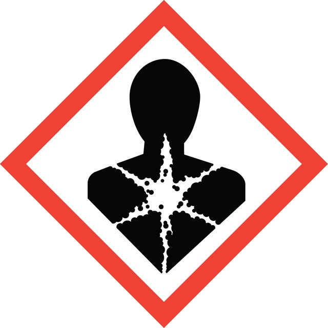
Hazard Classifications
STOT RE 1 Inhalation
target_organs
Lungs
存储类别
6.1C - Combustible acute toxic Cat.3 / toxic compounds or compounds which causing chronic effects
wgk
WGK 1
flash_point_f
Not applicable
flash_point_c
Not applicable
ppe
dust mask type N95 (US), Eyeshields, Gloves
Ching-Hwa Ho et al.
ACS applied materials & interfaces, 5(6), 2269-2277 (2013-03-05)
The surface formation oxide assists of visible to ultraviolet photoelectric conversion in α-In2Se3 hexagonal microplates has been explored. Hexagonal α-In2Se3 microplates with the sizes of 10s to 100s of micrometers were synthesized and prepared by the chemical vapor transport method
Thirumaleshwara N Bhat et al.
Journal of nanoscience and nanotechnology, 13(1), 498-503 (2013-05-08)
The thermal oxidation process of the indium nitride (InN) nanorods (NRs) was studied. The SEM studies reveal that the cracked and burst mechanism for the formation of indium oxide (In2O3) nanostructures by oxidizing the InN NRs at higher temperatures. XRD
V M Katerynchuk et al.
Journal of nanoscience and nanotechnology, 12(11), 8856-8859 (2013-02-21)
The photosensitive In2O3-p-InSe heterostructures in which the In2O3 frontal layer has a nanostructured surface were investigated. The photoresponse spectra of such heterostructures are found to be essentially dependent on surface topology of the oxide. The obtained results indicate that the
Vahid A Akhavan et al.
ChemSusChem, 6(3), 481-486 (2013-02-13)
Thin-film photovoltaic devices (PVs) were prepared by selenization using oleylamine-capped Cu(In,Ga)Se2 (CIGS) nanocrystals sintered at a high temperature (>500 °C) under Se vapor. The device performance varied significantly with [Ga]/[In+Ga] content in the nanocrystals. The highest power conversion efficiency (PCE) observed
Annick Bay et al.
Optics express, 21 Suppl 1, A179-A189 (2013-02-15)
In this paper the design, fabrication and characterization of a bioinspired overlayer deposited on a GaN LED is described. The purpose of this overlayer is to improve light extraction into air from the diode's high refractive-index active material. The layer
我们的科学家团队拥有各种研究领域经验,包括生命科学、材料科学、化学合成、色谱、分析及许多其他领域.
联系客户支持