
产品名称
单层石墨烯薄膜, 1 cm x 1 cm on quartz, avg. no. of layers, 1
Quality Segment
form
film
feature
avg. no. of layers 1
resistance
600 Ω/sq
L × W × thickness
1 cm × 1 cm × (theoretical) 0.345 nm, monolayer graphene film, 1.25 cm × 1.25 cm × 525 μm, quartz substrate
General description
Graphene is a unique one atom thick, two dimensional allotrope of carbon. Among all the synthesis technique, chemical vapor deposition of graphene on various substrates is the most promising route for the large scale production of good quality graphene. Graphene deposited on dielectric surface may exhibit better performance in graphene based FETs. Graphene deposited on quartz may be deposited by direct chemical vapor deposition via a sacrificial copper film.
Growth Method: CVD synthesis
Transfer Method: Clean transfer method
Quality Control: Optical Microscopy & Raman checked
Size: 1 cm x 1 cm
Appearance (Color): Transparent
Transparency: >97%
Appearance (Form): Film
Coverage: >95%
Number of graphene layers: 1
Thickness (theoretical): 0.345 nm
FET Electron Mobility on Al2O3: 2; 000 cm2/V·s
FET Electron Mobility on SiO2/Si (expected): 4; 000 cm2/V·s
Sheet Resistance: 600 Ohms/sq.
Grain size: Up to 10 μm
Substrate Quartz
Size: 1.25 cm x 1.25 cm
Flatness: bow: 20μm; warp: 30μm
Roughness:6 angstroms (on the polished side)
Surface: Double side polished
Application
Graphene may be extensively incorporated in several applications, such as; nanoelectronics, fuel cells, solar cell, photovoltaic devices, in biosensing, optical biosensors, MEMS, NEMS, field effect transistors (FETs), chemical sensors, nanocarriers in biosensing assays., 4
Still not finding the right product?
Explore all of our products under 单层石墨烯薄膜
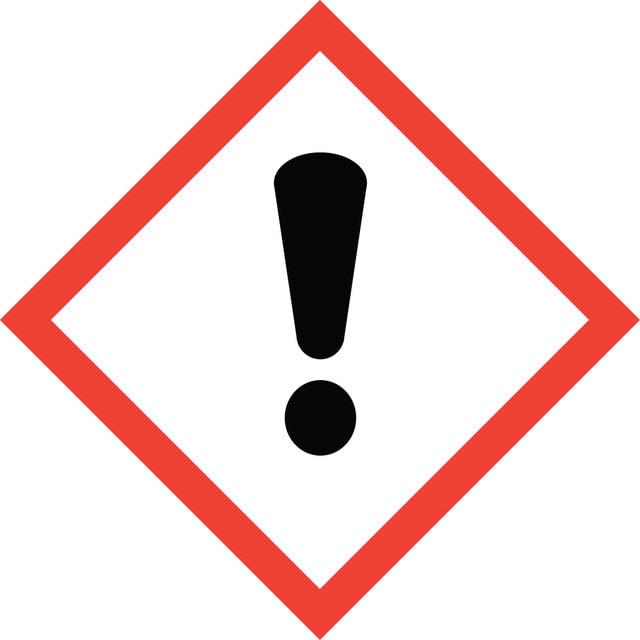
signalword
Danger
hcodes
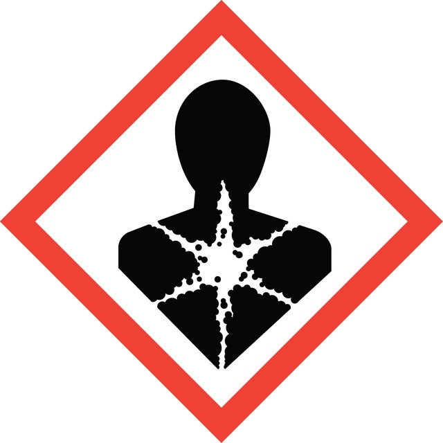
Hazard Classifications
Carc. 1B - Eye Irrit. 2 - STOT RE 1 Inhalation - STOT SE 3
target_organs
Lungs, Respiratory system
存储类别
6.1D - Non-combustible acute toxic Cat.3 / toxic hazardous materials or hazardous materials causing chronic effects
wgk
WGK 3
flash_point_f
Not applicable
flash_point_c
Not applicable