Precise Nanoparticles for Optoelectronics
Introduction
Inorganic nanomaterials are tunable by size, shape, structure, and/or composition. Advances in the synthesis of well-defined nanomaterials have enabled control over their unique optical, electronic, and chemical properties stimulating tremendous interest across a wide range of disciplines. This article illuminates some of the recent research advances of inorganic nanoparticles (NPs) in optoelectronics applications.
Inorganic Nanostructures and Properties
Since the intrinsic characteristics and relevant applications of nanoparticles are closely related to their size, shape, and surface properties, great efforts have been devoted to the controlled synthesis of nanoparticles. Key properties of nanoparticles (such as gold and silver) can thus be tailored by altering their physical geometries. Numerous publications have addressed the unique properties exhibited by variously metal nanoparticle shapes, including gold nanospheres (Figure 1),1 nanorods,2 nanoprisms,3 nanocubes,4 and nanowires.5 The optical properties, including optical resonance wavelengths, extinction cross-section, relative contribution of scattering to the extinction, can be tuned for different applications. Spherical nanoparticles offer resonance wavelengths in the visible region, while nanoshell and nanorod resonances are shifted into the Near Infrared (NIR) region. Moreover, nanoshells and nanorods optical properties are enhanced by altering the core-shell radius and aspect ratio, respectively.
Optical properties are conferred by the interaction of light with electrons on the metal nanoparticle surface. At a specific wavelength (frequency) of light, the collective oscillation of electrons on the metal nanoparticle surface causes a phenomenon called surface plasmon resonance, which results in a strong extinction of light. The particular wavelength, or frequency, of light at which this occurs is strongly dependent on the nanoparticle size, shape, surface, and agglomeration state. This strongly enhanced surface plasmon resonance of nanoparticles (especially within the optical frequency range) allows them to be excellent scatterers and absorbers of visible light. This phenomenon, coupled with advances in nanomaterial syntheses,6 surface conjugation,7 and self-assembly,8 has advanced the use of precise plasmon resonant nanostructures for optical,9 optoelectronics, and biodiagnostic applications.10
Organic Photovoltaic (OPV) Devices
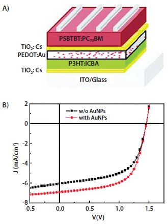
There have been numerous reports on power conversion efficiency (PCE) enhancement of organic photovoltaic devices using metal nanoparticles. In 2011, an international team of researchers led by Professor Yang at UCLA reported 20% efficiency of existing OPVs using gold nanoparticles (Figure 2).11 They were the first to fabricate a plasmonic-enhanced tandem OPV cell and show the plasmonic effect has future potential for OPV research. In another approach, Chia-Ling Lee and co-workers at the National Chiao Tung University incorporated gold nanoparticles into the anodic buffer layer in an attempt to trigger localized surface plasmon resonance (LSPR) which increased the PCE from 3.57% to 4.2%.12 It was determined that the improved performance resulted from local enhancement of the electromagnetic field surrounding the gold nanoparticles.

Figure 2.A) Schematic of plasmonic polymer tandem solar cell, ITO/TiO2:Cs/P3HT: IC60BA/PEDOT:Au/TiO2:Cs/PSBTBT:PC70BM/MoO3/Al. B) The J–V characteristics of the tandem solar cells under AM1.5G 100 mW·cm-2 illumination.11
Organic Field Effect Transistor (OFET)/Organic Thin-Film Transistor (OTFT) Materials
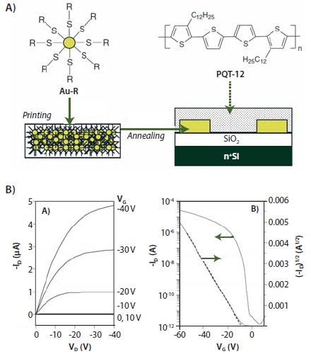
The incorporation of inorganic nanoparticles has been investigated in organic thin film transistor (OTFT) devices. Brian Chiang and co-workers at the Xerox Research Center of Canada have solution-deposited metal nanoparticles (primarily gold) to electrodes in a bottom-contact OTFT device using polyquaterthiophene (PQT-12) as an organic semiconductor, as shown in Figure 3.13 The work was carried out at lower temperatures to ensure compatibility with commercially available plastic substrates. The switching capabilities were found to be comparable with analogous devices using more intensive and costly processes such as vacuum deposition of the gold electrodes.

Figure 3. A) Schematic depiction of printing gold source and drain electrodes using gold nanoparticles for a bottom-contact OTFT device using PQT-12 as a semiconductor. B) Plot of drain current ID vs. source-drain voltage VD as a function of gate voltage VG for an example OTFT with printed source and drain electrodes with channel length 240 μM and width of 2,200 μM.13
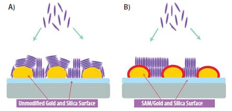
Yu-Tai Tao and Chiao-Wei Tseng at the Institute of Chemistry in Taiwan have integrated surface functionalized gold nanoparticles into the conducting channel of a pentacene film-based OFET device.14 The selfassembly of the gold nanoparticles was shown to dramatically influence the crystallinity and morphology of the thermally evaporated pentacene (698423) films most likely due to the strong metalpentacene interaction (Figure 4). Electric bistability was observed on account of the charge-holding gold nanoparticles; hence, the feasibility of metal nanoparticles to serve as a floating gate in the transistor/ memory function was demonstrated.14

Figure 4.Schematic diagram showing pentacene molecules deposited on silicon substrate decorated with A) Unmodified Gold NPs and B) SAM-modified Gold NPs.14 Reprinted with permission from ACS.
Molecular Electronics/Non-Volatile Memory
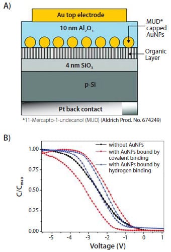
Srinivasan and co-workers, at the National University in Singapore, have made significant steps toward the enhancement of non-volatile memory and ultimately the realization of nanoparticle-based electronic devices. They have reported the fabrication of a metal-insulatorsemiconductor (MIS) device (Figure 5) by the covalent attachment of functionalized gold nanoparticles onto a silica substrate using gantrez polymer as a surface modifier.15 The enhanced stability of the immobilized nanoparticles was tested by sonication. No noticeable change was observed by field emission scanning electron microscopy (FESEM). The MIS device showed well-defined cyclic voltammetry (CV) hysteresis curves, which imply a good memory effect and good retention characteristics up to 20,000 s. Also, the voltage shift was 1.64 V at a swapping voltage of ±7 V.

Figure 5. A) MIS device configuration for the immobilized Au nanoparticles. B) Normalized C–V characteristics at 100 kHz obtained by biasing the top electrodes at ±6 V for control sample (without gold nanoparticle) and with gold nanoparticle.15 Reprinted with permission from ACS.
Optoelectronics—Fluorescent Nanocrystals
As the world becomes progressively electronic, the efficiency of electronic capture, storage, and presentation of images is continually advancing. As a result, the ability to cost-effectively mass-produce highperformance image sensors and displays is an ongoing challenge. A technology that promises to meet these needs features fluorescent nanocrystals, also known as quantum dots (QDs), which are nanoscale semiconductor crystals, usually held in a liquid suspension. Because of the promise of improved color quality from their light emission, combined with power-efficient operation and cost-effective solutionbased processing, fluorescent nanocrystals continue to attract intense academic and commercial interest.
Fluorescent nanocrystals owe their unique light emission and absorption characteristics to their miniature size and quantum confinement. By simply changing the particle size or, in our case the composition, it is possible to tune their bandgaps, emission colors, and absorption spectrum throughout the visible and infrared wavelengths. Because the absorption is broadband, fluorescent nanocrystals are promising for photodetector and photovoltaic applications. Also, their emission is narrow, making them extremely useful materials for displays, lighting applications, optical labeling and barcoding.
Cho et al.16 have demonstrated a solution-processable active-matrix array (large area) of red light-emitting devices (LEDs) based on CdSe/CdS/ZnS fluorescent nanocrystals combined with both organic and inorganic semiconductor layers (Figure 6).

Figure 6. A) Device structure (left) and cross-sectional TEM image (right) of the QD-LED. TFB, poly[(9,9-dioctylfluorenyl-2,7-diyl)-co-(4,4′-(N-(4-sec-butylphenyl))diphenylamine)]. Scale bar, 100 nm. B) Schematic structure with associated energy band diagram. The QD and TiO2 energy bands were determined from UPS and optical absorption measurements.16
Summary and Future Directions
The symbiosis of organic and inorganic nanomaterials can have some groundbreaking effects on solving some of the research challenges in materials science. Commercially, great care is often taken to ensure in the purity and correct specifications of available organic materials. However, this is not always the case in funcitionalized nanomaterials. Highly precise inorganic nanomaterials are becoming an integral part of many research groups worldwide, and as a result we will witness rapid advances in materials science.
Materials
References
To continue reading please sign in or create an account.
Don't Have An Account?