
651486
砷化镓
(single crystal substrate), <100>, diam. × thickness 2 in. × 0.5 mm
别名:
Gallium monoarsenide
登录并加购,请在购物车里查看协议价、货期和发货地。
选择规格
变更视图
关于此项目
线性分子式:
GaAs
化学文摘社编号:
分子量:
144.64
NACRES:
NA.23
PubChem Substance ID:
UNSPSC Code:
12352300
EC Number:
215-114-8
MDL number:
form
(single crystal substrate)
resistivity
≥1E7 Ω-cm
diam. × thickness
2 in. × 0.5 mm
density
5.31 g/mL at 25 °C (lit.)
semiconductor properties
<100>
SMILES string
[Ga]#[As]
InChI
1S/As.Ga
InChI key
JBRZTFJDHDCESZ-UHFFFAOYSA-N
General description
未掺杂的(Si 型半导体),蚀坑密度 <5×104cm-2,生长技术为液封直拉法和水平布里奇曼法
迁移率 ≥4500cm2 · V-1 · S-1
Physical form
cubic (a = 5.6533 Å)
Still not finding the right product?
Explore all of our products under 砷化镓
signalword
Danger
hcodes
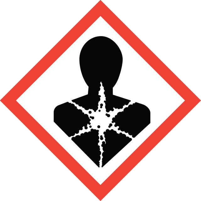
Hazard Classifications
Carc. 1B - Repr. 1B - STOT RE 1
target_organs
Respiratory system,hematopoietic system
存储类别
6.1A - Combustible acute toxic Cat. 1 and 2 / very toxic hazardous materials
wgk
WGK 3
flash_point_f
Not applicable
flash_point_c
Not applicable