跳转至内容
Merck
CN

703192

氧化铟锡涂层玻璃载玻片,方形

surface resistivity 8-12 Ω/sq

别名:

ITO, ITO 涂覆的正方形玻片

登录 查看组织和合同定价。

选择尺寸

变更视图

关于此项目

线性分子式:
In2O3 · (SnO2)x
化学文摘社编号:
NACRES:
NA.23
PubChem Substance ID:
UNSPSC Code:
12352103
MDL number:
技术服务
需要帮助?我们经验丰富的科学家团队随时乐意为您服务。
让我们为您提供帮助


Quality Level

description

Substrates and Prefab Devices, slide

surface resistivity

8-12 Ω/sq

L × W × thickness

25 mm × 25 mm × 1.1 mm

transmittance

84% (nominal at 550nm)

refractive index

n20/D 1.517

density

1.200 g/cm3

SMILES string

O=[Sn]=O.O=[In]O[In]=O

InChI

1S/2In.5O.Sn

InChI key

LNNWKAUHKIHCKO-UHFFFAOYSA-N

General description

氧化铟锡(ITO)广泛用作透明导电氧化物。其主要特征是导电性、光学透明性,并且易于沉积成薄膜。
ITO 涂层厚度为 1,200-1,600Å
衬底:未抛光浮法玻璃,SiO2 钝化(200-300Å)

Application

ITO玻璃载玻片可用作通过聚合物半导体与有机发光二极体(OLED)混合材料制备聚合物太阳能电池的基板。ITO基板也可用于通过印刷工具蚀刻基板表面来对透明加热器阵列进行设计。ITO盖玻片可用于封闭的数字微流体装置,并可用作显示器和其他光电装置中的透明电极。已报道的一些其他可能用途包括:
  • 在ITO覆盖的玻璃基底上制备真黑素样品。
  • 用于光束偏转(OBD)传感的液体电池的界面窗口包含一个20nm厚的氧化铟锡薄膜。
  • 在ITO导电玻璃上形成介孔TiO2 薄膜。


Still not finding the right product?


wgk

WGK 3

flash_point_f

Not applicable

flash_point_c

Not applicable

ppe

dust mask type N95 (US), Eyeshields, Gloves

pictograms

Health hazard

signalword

Danger

hcodes

Hazard Classifications

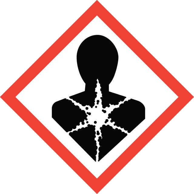
STOT RE 1 Inhalation

target_organs

Lungs

存储类别

6.1C - Combustible acute toxic Cat.3 / toxic compounds or compounds which causing chronic effects


历史批次信息供参考:

分析证书(COA)

Lot/Batch Number

没有发现合适的版本?

如果您需要特殊版本,可通过批号或批次号查找具体证书。

已有该产品?

在文件库中查找您最近购买产品的文档。

访问文档库


实验方案

Selenium's roles range from essential dietary element to semiconductor in advanced applications like xerography.

商品

A transparent conductive electrode (TCE) is an essential component of various optoelectronic devices such as solar cells, liquid-crystal displays (LCD), light-emitting diodes (LED), and touch screens.

Progress in solution-processed functional materials leads to thin-film optoelectronic devices for industrial and consumer electronics.

Professor Shinar highlights low-cost, disposable sensor configurations in organic and hybrid electronics for healthcare applications.

查看所有文章

Keith A Brown et al.
Proceedings of the National Academy of Sciences of the United States of America, 110(32), 12921-12924 (2013-07-19)
Scanning probe lithography (SPL) is a promising candidate approach for desktop nanofabrication, but trade-offs in throughput, cost, and resolution have limited its application. The recent development of cantilever-free scanning probe arrays has allowed researchers to define nanoscale patterns in a
Myungjae Yang et al.
Small (Weinheim an der Bergstrasse, Germany), 14(25), e1800885-e1800885 (2018-05-29)
A method is developed to directly map nanoscale "noise-source switching" phenomena during the optoelectronic switching of phase-separated polymer nanocomposites of tetrathiafulvalene (TTF) and phenyl-C61 -butyric acid methyl ester (PCBM) molecules dispersed in a polystyrene (PS) matrix. In the method, electrical
Preparation of non-annealed anatase TiO< sub> 2</sub> film on ITO substrate by anodizing in hot phosphate/glycerol electrolyte for dye-sensitized solar cells.
Tsuji E, et al.
Materials Letters, 91, 39-41 (2013)


全球贸易项目编号

货号GTIN
703192-10PAK04061832821344