
form
liquid
color
blue
pH
>9
正在寻找类似产品? 访问 产品对比指南
General description
Improved standard electroless nickel plating composition specific for making ohmic contacts to silicon and other semiconductor materials.
Advantages:
An improved electroless nickel plating solution (Brenner type) formulated for semiconductor use. Specifically, it is designed to deposit nickel uniformly and at equal plating rates on both p- and n- type silicon. The composition of this product is based upon ions of nickel complexes and hypophosphite with stabilizers. Only high purity chemicals are used. The plating solution is a stable product ready to use without the need for additions or mixing. Transene Electroless Nickel Plating Ammonia Type operates under conditions of a catalytic oxidation-reduction reaction between nickelous and hypophosphite ions. The chemical reaction is essentially a two-step process occurring simultaneously.
H2PO2- + H2O --> H2PO3 - + 2H+ + 2e- (1)
Ni2+ + 2e- --> Ni (2)
Nickel is deposited containing about 1% phosphide which improves the physical properties of the metalization.
The plating solution has an optimized standard electrode potential of 0.44 volts. The electrode characteristics help to regulate the difference in electronegativity between p- and n- type silicon relative to the potential of the nickel complex ions. Thus the rate of deposition of nickel on p- and n- silicon is equalized. The deposition on p- and n- type silicon is 2,000 Å/minute at 90 °C.
Advantages:
- Stable, ready to use
- Plates uniformly on p- and n- type silicon
- Offers excellent adhesion and solderability
- Plates on silicon, germanium, gallium arsenide
- Produces quality electrical contacts on p- and n- type silicon
An improved electroless nickel plating solution (Brenner type) formulated for semiconductor use. Specifically, it is designed to deposit nickel uniformly and at equal plating rates on both p- and n- type silicon. The composition of this product is based upon ions of nickel complexes and hypophosphite with stabilizers. Only high purity chemicals are used. The plating solution is a stable product ready to use without the need for additions or mixing. Transene Electroless Nickel Plating Ammonia Type operates under conditions of a catalytic oxidation-reduction reaction between nickelous and hypophosphite ions. The chemical reaction is essentially a two-step process occurring simultaneously.
H2PO2- + H2O --> H2PO3 - + 2H+ + 2e- (1)
Ni2+ + 2e- --> Ni (2)
Nickel is deposited containing about 1% phosphide which improves the physical properties of the metalization.
The plating solution has an optimized standard electrode potential of 0.44 volts. The electrode characteristics help to regulate the difference in electronegativity between p- and n- type silicon relative to the potential of the nickel complex ions. Thus the rate of deposition of nickel on p- and n- silicon is equalized. The deposition on p- and n- type silicon is 2,000 Å/minute at 90 °C.
Application
Silicon surfaces must be clean and etched in Buffer-HF or HF solution to remove oxide, rinsed and stored in alcohol. On polished silicon wafers, plate 1000-2000 A of electroless nickel; greater thickness on lapped silicon surfaces. The deposited nickel can be sintered into silicon at 500 °C to 750 °C to promote adhesion and ohmic contact. A second nickel deposit is generally required.
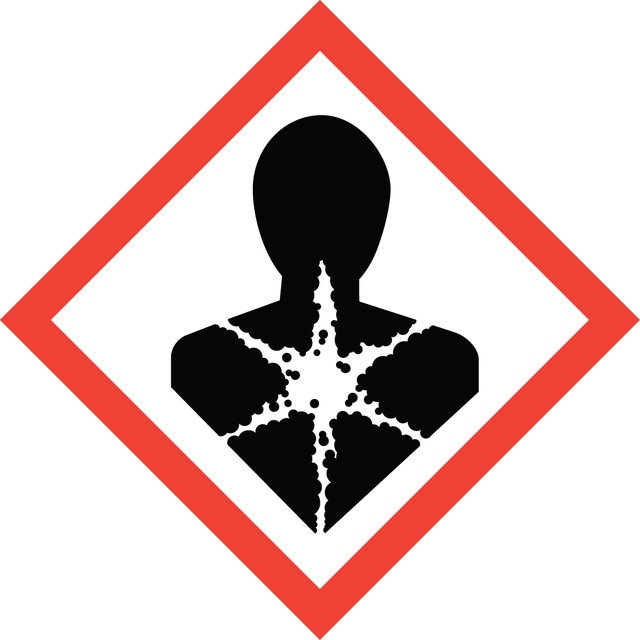

signalword
Danger
Hazard Classifications
Aquatic Chronic 2 - Carc. 1A Inhalation - Eye Irrit. 2 - Muta. 2 - Repr. 1B - Resp. Sens. 1 - Skin Irrit. 2 - Skin Sens. 1 - STOT RE 1 - STOT RE 2 Inhalation
target_organs
Lungs
wgk
WGK 3
法规信息
新产品
此项目有
我们的科学家团队拥有各种研究领域经验,包括生命科学、材料科学、化学合成、色谱、分析及许多其他领域.
联系客户支持