Organic Field Effect Transistors Based on DNTT
Introduction
Highly extended polyacenes such as pentacene and naphthacene have been essential organic semiconductors for high-performance organic field-effect transistors (OFETs). In fact, pentacene-based OFETs have driven the field of organic electronics in the last decade.1 In general, the carrier mobility of polyacenes is enhanced by increasing the number of fused aromatic rings. However, large polyacenes, such as hexacene2 and heptacene, without bulky protecting substituents are not chemically stable and therefore, devices prepared from these are less stable under ambient conditions, preventing their practical use in device applications. One approach to avoid such instability in simple hydrocarbon-based acenes has been to incorporate heteroaromatics, such as thiophenes, into the acene structure affording thienoacenes, which in many cases has shown good stability and high carrier mobility.3
Among the range of thienoacene-based organic semiconductors, materials with an internal thieno[3,2-b]thiophene substructure, such as [1]benzothieno[3,2-b][1]benzothiophene (BTBT)4 and dinaphtho[2,3-b:2',3'-f]thieno[3,2-b]thiophene (DNTT)5 (Figure 1) have shown the best p-channel organic semiconductors for OFET applications in terms of high mobility, air stability, and good reproducibility. Herein, we summarize the representative materials in terms of materials diversity, synthesis, OFET performance, packing structures in the solid state, and applications.

Figure 1.Molecular structures of BTBT, DNTT (Product No. 767638) and related organic semiconductor derivatives (Product Nos. 767611, 767646 and 767603).
Materials and Synthesis
The smallest molecular framework in this class is BTBT, which has been extensively studied and utilized as a core structure for liquid crystal materials. However, BTBT and its derivatives had not been examined as an active material in the organic field-effect transistor until 2006 when its 2,7-diphenyl derivative was reported to be a superior organic semiconductor showing mobility of up to 2.0 cm2 V–1 s–1.4 Since then, several BTBT derivatives have been explored as organic semiconductors and most of the BTBT derivatives with substituents at 2- and/or 7- positions act as superior organic semiconductors with very high mobilities.6
With these fruitful results on the BTBT-based organic semiconductors, it is quite natural to extend its conjugation system in order to search for new superior materials. The π-extended analogues of BTBT in a linear manner, DNTT5 and dianthra[2,3-b:2',3'-f]thieno[3,2-b]thiophene (DATT)7,8 were synthesized in 2007 and 2011, respectively. For the syntheses of these π-extended analogues, the iodine-promoted thieno[3,2-b]thiophene formation reaction from the corresponding o-bis(methylthio)stilbene type precursors is the key (Scheme 1),5 and in fact, various DNTT derivatives including alkyl and phenyl substituents can be synthesized analogously.9

Scheme 1.Iodine-promoted thieno[3,2-b]thiophene formation from o-bis(methylthio)stilbene precursors.
Performances of OFETs
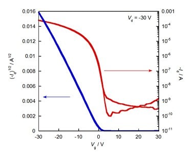
Despite their π-extended molecular framework like ordinary acene compounds, the BTBT and DNTT derivatives have low-lying HOMO energy levels (< –5.2 eV) relative to those of acenes with the same number of aromatic rings, owing to the inserted the thieno[3,2-b]thiophene substructure.10 The low-lying HOMO energy level contributes to the stability of the materials themselves and their thin-film transistors, and in fact, OFET derived from this class of compounds as an active layer can operate in ambient conditions without degradation. Typical transfer characteristics of DNTT-based OFETs fabricated on Si/SiO2 substrate by vacuum deposition is shown in Figure 2, where very low off-current, small hysteresis, and sharp turn-on behavior are noticeable. Table 1 summarizes the characteristics of thin-film devices with some representative BTBT, DNTT, and related materials as an active semiconducting layer. Regardless of the materials, the extracted mobilities are quite high (> 1.0 cm2 V–1s–1) with large on/off current ratios.

Figure 2.Typical transfer characteristics of the DNTT-based OFET devices fabricated on Si/SiO2 substrate.
Applications of OFETs Device
With their superior characteristics and stability, these materials have been employed into i) various FETs with new device architectures other than the conventional thin-film transistor configuration, ii) new processing methods for device fabrications, and iii) state-of-the art flexible organic thin-film transistor (OTFT) circuits.
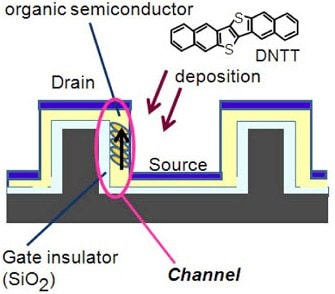
Vapor-grown single crystals of DNTT used to develop single crystal FETs (SC-FETs) led DNTT to be recognized as a high-performance organic semiconductor with a record high mobility up to 8.3 cm2 V–1s–1.13 DNTT has a relatively small anisotropy of the transport properties: the anisotropy ratio of mobility measured in the different crystallographic directions on the single crystals is in a range of 1.3–1.6 (Figure 3), which corroborates the isotropic (two-dimensional) electronic structure of DNTT expected from its crystal structure (vide infra).14 Another unconventional device architecture examined is the three-dimensional (3D)-OFET that can afford an extremely high ratio of the channel width (W) and length (L), enabling to modulate very high current density per area (Figure 4).15 An additional advantage of the 3D-OFET is that devices can be made with extremely short L down to 1 µM, which gives very high response speed of up to several tens of MHz even on the flexible substrate.16

Figure 3.Angular dependence of the field-effect mobility of DNTT-based SC-OFET. Adapted from Reference 14 with permission (© 2009 American Institute of Physics).

Figure 4.Illustration of cross-sectional view of the typical 3D-OFET. Adapted from Reference 15 with permission (© 2009 American Institute of Physics).
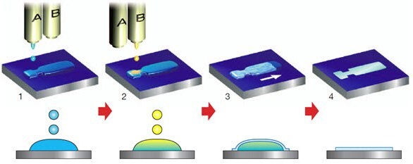
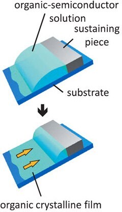
As another example of applications, highly soluble alkylated BTBT can be solution processable. Using a double-shot inkjet method, two types of inks composed of an anti-solvent and a solution of C8-BTBT, respectively, are inkjeted consecutively in a controlled manner to form single crystalline thin films directly on the substrate (Figure 5). OFETs with the single crystalline thin films as an active layer showed extremely high mobility, 16.4 cm2 V–1s–1 on average and the maximum value of 31.3 cm2 V–1s–1.17 Another innovative solution processing method developed by using C8-BTBT, the so-called “directing crystallization” is affording crystalline thin films of the organic semiconductor on the substrate directly; by controlling the drying process of organic semiconductor solution sustained on the substrate, single crystal-like thin films can grow in a certain direction (Figure 6), and the resulting high-quality crystalline film of C8-BTBT can act as the semiconducting channel affording high performance OFETs with mobility as high as 5 cm2 V–1s–1.18 This “directing crystallization” method can be applied to the formation of C10-DNTT thin film, which affords OFETs with much better mobility of up to 12 cm2 V–1s–1.19 The method also allows depositing the plural crystalline thin films simultaneously on the substrate, enabling to fabricate transistor matrix, which are now examined as the back plane of active matrix liquid crystalline displays.20

Figure 5.Inkjet printing process of organic single-crystal thin films. Anti-solvent ink (A) is first inkjet-printed (step 1), followed by solution ink (B) overprinted sequentially to form intermixed droplets confined to a predefined area (step 2). Semiconducting thin films grow at liquid–air interfaces of the droplet (step 3) before the solvent fully evaporates (step 4). Adapted from Reference 17 with permission (© 2011 Nature Publishing Group).

Figure 6.Schematic of the method of oriented growth of C8-BTBT crystalline thin film from its solution sustained on the substrate. Adapted from Reference 18 with permission (© 2009 The Japan Society of Applied Physics).
In addition to the fundamental research, application-oriented studies on DNTT-based OFET circuits are also reported. For the practical usage of OTFT circuits, lowering the operation voltage, flexibility of the circuits, and good stability/reliability are important issues. The DNTT OFETs fabricated on the AlOx/SAM dielectrics developed by Klauk and coworkers meet all these criteria (Figure 7).21 The transistors can operate less than 5 V with mobility as high as 2 cm2 V–1s–1 on flexible plastic substrates or even on paper (Figure 8),22 and their long-term stability both under the shelf-life conditions and bias-stressed conditions are also described. Furthermore, thermal stability of the DNTT-OFETs up to 150 °C for 20s is also confirmed, which indicates that standard medical sterilization procedure can be applied to DNTT-OFETs, paving the way to practical medical application of OFETs.23

Figure 7.Cross section and photograph of a DNTT TFT on a flexible PEN substrate. Adapted from Reference 21 with permission (© 2010 Wiley).

Figure 8.a) Photograph of a 5-Euro note with arrays of organic transistors and circuits, b) Photograph of an individual transistor on a banknote. Adapted from Reference 22 with permission (© 2011 Wiley).
Packing and Electronic Structures in the Solid State
The excellent properties in OFET devices listed in Table 1 are rationalized by the packing structure of the materials in this class. They typically possess edge-on molecular orientation on the substrate, and their in-plane structures are characterized as highly interactive, two dimensional herringbone packing (Figure 9). In general, the herringbone packing contains two types of intermolecular pairs; edge-to-edge pairs (stacking pairs) in the crystallographic a-axis direction and edge-to-face pairs in the crystallographic b-axis directions. Compared to the latter edge-to-face pairs, intermolecular orbital coupling in the former pairs tends to be smaller in conventional acene-based materials because of less effective intermolecular contacts through the molecular edges. For the packing structure of the BTBT- and DNTT-based materials, on the other hand, sulfur atoms at the thienothiophene moiety in the middle of the ladder-shaped π-extended systems can effectively interact intermolecularly. Furthermore, the large HOMO coefficients on the sulfur atoms are also beneficial to enhance intermolecular orbital overlaps. As a result, a well-balanced two-dimensional electronic structure is realized in the semiconducting channel regardless of the compounds in this class.

Figure 9.Packing structure of DNTT: (a) edge-on molecular orientation on the substrate, (b) herringbone molecular arrangement in the in-plane direction, and (c) schematic representation of intermolecular HOMO overlap in the herringbone structure of DNTT.
Summary
In this article, recent developments on the DNTT- and BTBT-based organic semiconductors are described. The characteristic features of the present organic semiconductors are: (i) good chemical and environmental stability originating from their low-lying HOMO energy levels; (ii) to afford high quality thin films suitable for thin film transistor application; and (iii) highly interactive solid state structure with two-dimensional strong intermolecular interaction in the solid state. All these features make the materials ideal organic semiconductors as active materials in OFETs. As many cutting-edge applications of the present organic semiconductors have recently been demonstrated, it is expected that further applications of these materials will be accelerated in future, and also the materials design strategy elucidated during the development of the DNTT- and BTBT- based organic semiconductors will stimulate to create new advanced organic semiconductors.
References
如要继续阅读,请登录或创建帐户。
暂无帐户?