ZnO Aggregates in Dye-Sensitized Solar Cells
Introduction
Solar energy, as the primary source of energy for all living organisms on Earth, is considered the ultimate solution to the energy and environmental challenge as a carbon-neutral energy source. Many photovoltaic devices that fulfill the energy conversion from sunlight to electricity have already been developed over the past five decades. However, their widespread usage is still limited by two significant challenges; namely conversion efficiency and cost.1 One of the more traditional photovoltaic devices, single crystalline silicon solar cells were invented more than 50 years ago, currently make up 94% of the market. Single crystalline silicon solar cells operate on the principle of p-n junctions formed by joining p-type and n-type semiconductors. The electrons and holes are photogenerated at the interface of p-n junctions, separated by an electrical field across the p-n junction, and collected through the external circuits. Unfortunately, single crystalline silicon solar cells suffer from both high materials costs and energy-intensive production processes. Amorphous thin film silicon is a good replacement candidate because the defect energy levels can be controlled by hydrogenation and the band gap can be reduced so that the light absorption efficiency can be much higher than that of crystalline silicon. However, amorphous silicon tends to be unstable and can lose up to 50% efficiency within the first one hundred hours. Bridging the gap between single crystalline silicon and amorphous silicon is the polycrystalline silicon film, for which a conversion efficiency of around 15% is obtained. Compound semiconductors such as gallium arsenide (GaAs, Prod. No. 329010), cadmium telluride (CdTe, Prod. No. 716669) and copper indium gallium selenide (CIGS) have received much attention because they present a direct energy gap, can be doped to either p-type or n-type, have band gaps matching the solar spectrum, and possess high optical absorbance. These devices have demonstrated conversion efficiencies of 16-32%. Although photovoltaic devices built on silicon or compound semiconductors have been achieving high efficiency for practical use, they still require major breakthroughs to meet the long-term goal of very low cost ($0.40/kWh).2-6
Dye-sensitized solar cells (DSCs) based on oxide semiconductors and organic dyes have recently emerged as a promising approach to efficient solar energy conversion at a low cost. The DSCs are a photoelectrochemical system which incorporates a porous-structured oxide film with adsorbed dye molecules as the photosensitized anode (Figure 1a and Figure 1b). A platinum-coated silicon wafer acts as the counter electrode (i.e., cathode), and a liquid electrolyte that traditionally contains I-/I3 - redox couples serves as a conductor to electrically connect the two electrodes.7-12 Photons are captured by the dye monolayer, creating excitons that are rapidly split at the nanocrystallite surface of oxide film; electrons are injected into the oxide film and holes are released by the redox couples in the liquid electrolyte. Compared with conventional single crystal silicon-based or compound semiconductor thin film solar cells, DSCs are thought to be advantageous as a photovoltaic device possessing both practical high efficiency and cost effectiveness. To date, the most successful DSC was based on a TiO2 nanocrystalline film combined with ruthenium-polypyridine complex dye as first reported by O’Regan and Grätzel in 1991.13 A certified overall conversion efficiency of 11% was achieved on TiO2-RuL’(NCS)3 (namely “black dye”) system, in which the spectral response of the complex dye was extended to the nearinfrared region so as to absorb far more of the incident light.9,14-16 The porous nature of nanocrystalline TiO2 films drives their use in DSCs due to the high surface area available for dye molecule adsorption. Meanwhile, the suitable relative energy levels at the semiconductor-sensitizer interface, i.e., the position of the conduction band edge of TiO2 being lower than the excited-state energy level of the dye, allow for the effective injection of electrons from the dye molecules to the semiconductor.

Figure 1. A dye-sensitized solar cell based on an electrochemical system. (a) Schematic of the construction and operational principle of device, (b) SEM image of oxide (TiO2) electrode film with nanocrystallites (~20 nm in diameter), and (c) Electron transport in nanocrystalline oxide electrodes, in which photoexcited electrons are injected from the dye to the conduction band (denoted as “c.b.”) of the nanocrystallite (1), the dye is regenerated by electron transfer from a redox couple in the electrolyte (3), a recombination may take place between the injected electrons and the dye cation (2) or redox couple (4). (4) is normally believed to be the predominant loss mechanism. Electron trapping in the nanocrystallites (5) is also a mechanism that causes energy loss. LUMO and HOMO represent the lowest unoccupied molecular orbital and the highest occupied molecular orbital of the dye, respectively.9,15,17
The achievement of acceptable power conversion efficiencies instilled much confidence in the ability of DSCs to challenge the high costs of commercially available solar cells based on silicon or compound semiconductors. However, further increases in power conversion efficiency have been limited by the energy loss due to the recombination between electrons and either the oxidized dye molecules or electron accepting species in the electrolyte during the charge transport process (Figure 1c).18-20 Such a recombination originates predominately from the lack of a depletion layer on TiO2 nanocrystallite surface. This scenario becomes more evident when the thickness of photoelectrode film increases. A variety of approaches have been explored to overcome the electron recombination by using either one-dimensional nanostructures that provide a direct pathway for electron transport or using core-shell structures with an oxide coating on TiO2 (Prod. Nos. 718467, 677469) to minimize the recombination rate. Aside from those approaches, a series of methods that address the generation of photoexcited carriers by combining nanostructured films with optical effects (light scattering or optical confinement) has also been demonstrated to be effective in enhancing the light harvesting capability of the photoelectrode film so as to improve the DSC performance.21
Usami, Ferber, Luther, and Rothenberger et al. predicted that the optical absorption of dye sensitized TiO2 nanocrystalline films could be enhanced by admixing large sized TiO2 particles as the light scattering centers.22-24 The light scattering efficiency has been shown to correlate with both the size of the scattering centers and the wavelength of incident light.25 The scattering reaches a maximum when the size of the scattering centers is about kλ, where k is a constant and λ is the wavelength. Experimentally, it has been verified that the performance of DSCs can be significantly improved when the TiO2 nanocrystalline films are combined with large-sized SiO2 (Prod. No. 381276), Al2O3 (Prod. No. 202606), or TiO2 particles.26-30 By coupling a photonic crystal layer to conventional TiO2 nanocrystalline films for light scattering, Nishimura et al. and Halaoui et al. also succeeded in enhancing the light harvesting capability of the photoelectrode.31,32 However, the introduction of large-sized particles into nanocrystalline films has the unavoidable effect of lowering the internal surface area of the photoelectrode film. This serves to counteract the enhancement effect of light scattering on the optical absorption, whereas the incorporation of a photonic crystal layer may lead to an undesirable increase in the electron diffusion length and, consequently, increase the recombination rate of photogenerated carriers.
Some recent developments have been reported on the use of oxide nanocrystallite aggregates in DSCs.33-37 The oxide nanocrystallite aggregates demonstrated to be able to provide the photoelectrode with both a large surface area and efficient light scattering centers. As a result, very impressive enhancements in the overall conversion efficiency were achieved for ZnO-based DSCs.33,36 This review introduces the synthesis, characterization, and surface modification of ZnO aggregates, and shows the light scattering effect with these aggregates on the enhancement of the light harvesting efficiency (LHE) of photoelectrode, resulting in a very impressive increase in the conversion efficiency of the DSCs.
Enhanced Solar Cell Performance with Aggregates
Synthesis of ZnO Aggregates
ZnO aggregates can be synthesized by the hydrolysis of a zinc salt in a polyol medium and heating at 160 °C.36,38 Typically, zinc acetate dihydrate (0.01 mol, Prod. No. 379786) was added to diethylene glycol (DEG, 100 mL, Prod. No. H26456) with vigorous stirring. The mixture was rapidly heated in an oil bath at a rate of 10 °C/min. The reaction continued for about 8 h with continual stirring. As-obtained colloidal solution was then sequentially concentrated by 1) centrifugally separating the aggregates from the solvent, 2) removing the supernatant, and 3) redispersing the precipitate in ethanol (5 mL). The sample synthesized at 160 °C is denoted as Sample 1. For comparison, three more samples were also synthesized at temperatures of 170, 180, and 190 °C, denoted as Samples 2 through 4, respectively.
Fabrication of Photoelectrode Films
Photoelectrode films were fabricated on Fluorine-Tin-Oxide (FTO) glass using a drop-casting method. After the films dried, they were annealed at 350 °C for 1 h to remove any residual organic matter from the ZnO surface. The films were then sensitized by immersing them into 0.5 mm ethanolic solution of the ruthenium complex cis-[RuL2(NCS)2] (commercially known as N3 dye, Prod. No. 703206 )39,40 for approximately 20 min. The sensitization time was controlled strictly and limited to avoid the dissolution of surface Zn atoms and the formation of Zn2+/dye complexes, which might block the electron transport from the dye to semiconductor. The films were then rinsed with ethanol to remove the additional dye.
Morphology and Structure Characterization
The morphology of the film of ZnO aggregates (Sample 1) was characterized using a scanning electron microscope (SEM), as shown in Figure 2. It can be seen that the film is well-stacked with submicrometer-sized ZnO aggregates. These aggregates are polydisperse in size with diameters ranging from several tens to several hundreds of nanometers. The film therefore presents a highly disordered structure.
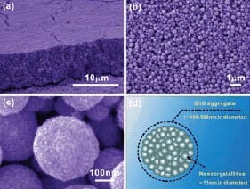
Figure 2. SEM images of ZnO film with aggregates synthesized at 160 °C (Sample 1) and a schematic showing the structure of individual aggregates.
A high magnification SEM image reveals that the ZnO aggregate is nearly spherical in shape and consists of packed nanocrystallites. In Figure 2d, the structure of an individual aggregate is schematically illustrated to further demonstrate the porous features provided due to the agglomeration of nanosized crystallites. This ZnO film was thought to adopt as a hierarchical structure in view of the architecture formed by secondary submicron-sized aggregates with primary nanocrystallites. Shown in Figure 3 are the SEM images of Samples 2 through 4. It is clear that, with increasing synthesis temperature, the degree of a spherical agglomeration of the nanocrystallites is gradually degraded. Sample 2, synthesized at 170 °C, is similar to Sample 1 and consists of aggregated ZnO nanocrystallites, but begins to show a slight destruction of the spherical shape (Figure 3a). Sample 3, synthesized at 180 °C, consists of partial aggregates, however most of the aggregates have lost their spherical shape (Figure 3b). As the synthesis temperature increases further to 190 °C, the obtained product (Sample 4) only presents dispersed nanocrystallites without any agglomeration (Figure 3c). X-ray diffraction (XRD) analysis revealed that all the samples were of a hexagonal wurtzite structure of ZnO. With XRD spectra and using the Scherrer equation,41 the primary nanocrystallite size was estimated to be about 15 nm in diameter for all the samples, i.e., there was no appreciable difference in the nanocrystallite size for these samples, despite the differences in synthesis temperature and morphology. Nitrogen sorption isotherms revealed that all four samples possessed almost equal specific surface area of approximately 80 m2/g.

Figure 3.SEM images of ZnO films with synthesis temperature of 170, 180, and 190 °C, corresponding to Samples 2 through 4, respectively.
Light Scattering of ZnO Aggregate Films
It was observed that Samples 1 through 4, i.e., the ZnO films synthesized at different temperatures as SEM images shown in Figures 2 and 3, demonstrated a difference in their transparency. This was a result of light scattering, as observed in the optical absorption spectra of the films upon dye sensitization (Figure 4). In the spectra, all the samples exhibit an intrinsic absorption with similar absorption intensity below 390 nm, caused by the ZnO semiconductor owing to electron transfer from the valence band to the conduction band. However, absorption at wavelengths above 400 nm vary significantly; such absorption originates from the dye molecules adsorbed on the ZnO surface and is related to the film structure. It has the highest intensity for Sample 1, less intensity for Samples 2 and 3, and the lowest intensity for Sample 4. It should be noted that only Sample 4 presents an absorption peak centered around 520 nm, corresponding to the visible t2→π* metal-to-ligand charge transfer (MLCT)39 in N3 dye but with a slight blue-shift due to the electronic coupling between N3 and ZnO, whereas the other three samples (1–3) show a monotonically increased absorption as the wavelength switches from visible to ultraviolet. The absorption spectra illustrate that the better aggregation of nanocrystallites induces more effective photon capturing in the visible region and also suggest the existence of a strong light scattering effect. Such an effect may partially scatter the incident light and weaken the transmittance of the films, thus resulting in the pseudo absorption deviating from that of adsorbed dye.
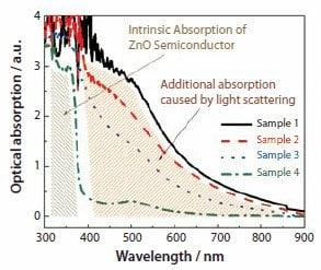
Figure 4.Optical absorption spectra of ZnO films of Samples 1 through 4.
Mie theory42,43 and Anderson localization of light44 provide the analytical description for the scattering of light by spherical particles and predict that resonant scattering may occur when the particle size is comparable to the wavelength of incident light. The aggregates within ZnO films are submicrometer-sized, and they are therefore particularly efficient scatterers for visible light, resulting in a significant increase in the light harvesting capability of the photoelectrode. Unlike large oxide particles, the ZnO aggregates are closely packed with nanocrystallites and therefore do not cause any loss in the internal surface area. It should be noted that the light scattering effect is usually imperceptible in conventional mesoporous TiO2 electrodes consisting of nanocrystallites smaller than 50 nm, because the size is far away from the wavelength of visible light; this is also the reason why Sample 4 presents a relatively weak absorption at the visible wavelengths.
Solar Cell Performance
The solar cells with as-prepared ZnO films were characterized by measuring the current–voltage behavior while irradiated by simulated AM 1.5 sunlight with a power density of 100 mW/cm2. Figure 5 shows typical current density versus voltage curves of the four ZnO samples. Sample 1, with near perfect aggregation, achieved the highest shortcircuit current density and, thus, the highest conversion efficiency, whereas Sample 4, consisting of only ZnO nanocrystallites, presented the lowest current density and the lowest energy conversion efficiency of all four samples. Table 1 summarizes the open-circuit voltages, the shortcircuit current densities, the fill factors, and the overall energy conversion efficiencies for all four samples. All samples possessed the same or similar open-circuit voltages of approximately 600 mV; however, the short-circuit current density varied significantly from 19 mA/cm2 for Sample 1 to 10 mA/cm2 for Sample 4. As a result, the energy conversion efficiency varied systematically from 5.4% for Sample 1 to 2.4% for Sample 4, decreasing as the degree of spherical aggregation decreased.
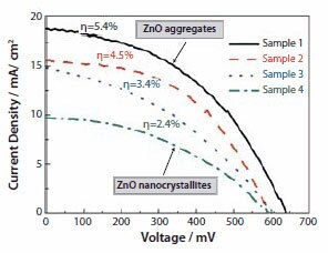
Figure 5.Photovoltaic response of ZnO films, Samples 1 through 4, while irradiated by standard AM 1.5 sunlight with an output power of 100 mW/cm2
*The conversion efficiency η and fill factor FF are calculated from η=Pout,max/Pinand FF=Pout,max/(VOC×ISC), where Pout,max is the maximum output power density, Pin is power density of the incident light, VOC is the open-circuit voltage, and ISC is the short-circuit current.
In view of the different optical absorption of these films, the variation in the solar cell conversion efficiency could be attributed to light scattering caused by a disordered film structure formed by the polydisperse aggregates. A disordered structure may lead to random multiple scattering in the film and, possibly, result in light localization due to the formation of traps for optical confinement. Photoinduced lasing emission on closely packed ZnO cluster films reported by Cao et al.45 and Wu et al.46 is one example that manifests the light scattering effect of highly disordered structure on the generation of light localization. In ZnO solar cells that consist of a photoelectrode film with aggregates, the light scattering may significantly extend the traveling distance of light within the photoelectrode and, thus, increase the probability of interaction between the photons and dye molecules. That means, the light scattering may result in an enhancement in the LHE of photoelectrode and therefore increases the conversion efficiency of solar cells. This is the reason that, in Figure 5, Sample 1 achieves a conversion efficiency of 5.4%, much higher than 2.4% obtained for Sample 4, the ZnO nanocrystalline film without light scattering.
Size Dependence of Conversion Efficiency
Size dependence of the solar cell conversion efficiency has been investigated to further demonstrate that the light scattering effect is closely related to the structure of the photoelectrode film, such as the average size and size distribution of the aggregates. For this purpose, both monodisperse and polydisperse ZnO aggregates were prepared. The method for the synthesis of polydisperse ZnO aggregates is a polyol-mediated precipitation method similar to that described above; however, the rate of heating was adopted to be different to control the degree of polydispersity. Specifically, a rapid heating at 10 °C/min was used to fabricate the polydisperse ZnO aggregates with a broad size distribution, while a rate of 5 °C/min was used to obtain the polydisperse aggregates with the relatively narrow size distribution. To synthesize monodisperse ZnO aggregates, an amount of stock solution was added into the reaction solution when the temperature reached 130 °C while the zinc acetate was completely dissolved. The stock solution was made of 5 nm ZnO nanoparticles prepared via a sol–gel approach and dispersed in the diethylene glycol with a concentration of about 10-3 M. The size of the aggregates could be adjusted by the amount of stock solution used. For example, 0.5 mL, 1 mL, 5 mL, 10 mL and 20 mL of stock solution gave monodisperse ZnO aggregates of 350 nm, 300 nm, 250 nm, 210 nm and 160 nm in diameter, respectively.
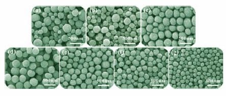
Figure 6.SEM images of ZnO films with aggregates different in size and size distribution. (a) and (b) Polydisperse aggregates, corresponding to groups 1 and 2, respectively, and (c) through (g) monodisperse aggregates, corresponding to groups 3 through 7, respectively.
To study the effects of the average size and size distribution of the aggregates on the solar-cell performance, a number of ZnO films with various structures were prepared and classified into seven groups, named group 1, 2, . . . through 7, in which the films in groups 1 and 2 were made of polydisperse ZnO aggregates and the others only included monodisperse aggregates. Figure 6 shows typical SEM images of all these film samples, where Figure 6a through 6g corresponds to the samples that belong to groups 1 through 7, respectively. One can see that the samples in group 1 consisted of polydisperse ZnO aggregates with diameter varying from 120 to 360 nm, while the samples in group 2 also consisted of polydisperse ZnO aggregates but with the diameter in the region of ~120–310 nm. The other samples were all monodisperse ZnO aggregates with average sizes varying from ~350 nm for group 3, ~300 nm for group 4, ~250 nm for group 5, ~210 nm for group 6, to ~160 nm for group 7.
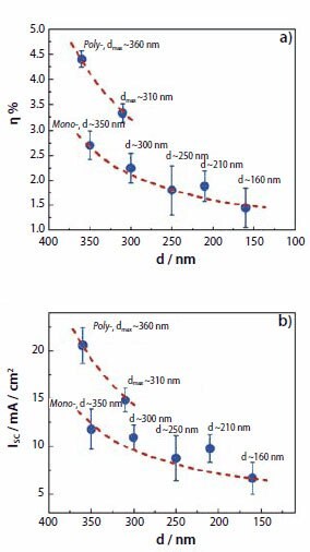
Figure 7.Dependence of (a) overall energy-conversion efficiency and (b) short-circuit current density on the size and size distribution of aggregates in dye-sensitized ZnO solar cells.
The solar-cell performance was characterized by measuring the current– voltage (I–V) behaviors of all of the samples when irradiated by a simulated AM 1.5 sunlight with a power density of 100 mW/cm2. The results are summarized in Figure 7, where Figure 7a shows the dependence of the energy-conversion efficiency on the diameter and size distribution of the ZnO aggregates, and Figure 7b indicates a similar trend for the short-circuit current density. It is clear that the photoelectrode films with polydisperse ZnO aggregates have both a higher energy-conversion efficiency and a larger short-circuit current density than the films with monodisperse ZnO aggregates. The electrode films consisting of polydisperse ZnO aggregates with a maximum diameter of 360 nm (samples in group 1) present the highest conversion efficiency of all the samples (4.4%), 33% higher than the efficiency of the polydisperse ZnO aggregates (3.3%) with the maximum diameter of 310 nm (samples in group 2), and 63% higher than the efficiency of monodisperse ZnO aggregates (2.7%) with an average size of ~350 nm (samples in group 3). Similarly, the largest short circuit current density of 21 mA/cm2, achieved for the polydisperse ZnO aggregates with the maximum diameter of 360 nm (samples in group 1), is 40% higher than that of 15 mA/cm2 for the polydisperse ZnO aggregates with the maximum diameter of 310 nm (samples in group 2), and 75% higher than that of 12 mA/cm2 for the monodisperse ZnO aggregate films (samples in group 3). As for the ZnO films with only monodisperse aggregates, one can see that the decrease in the size of the ZnO aggregates directly results in the degradation of the short-circuit current density from 12 mA/cm2 to 7 mA/cm2 and the energy-conversion efficiency from 2.7% to 1.5%. It has been demonstrated that the variation of conversion efficiency for the ZnO solar cell samples in different groups only results from the difference in photocurrent of the cells instead of open-circuit voltage or fill factor. Moreover, the photocurrent was basically related to either the dye adsorption amount determined by the internal surface area of the photoelectrode film or the propagation behavior of light within the photoelectrode film. A nitrogen sorption isotherm measurement revealed a same specific surface area, ~80 m2/g, for all these samples in different groups. The dye adsorption amount was probably not the reason for the difference in the short-circuit current density. Therefore, it was inferred that the film structures with differences in the aggregate size and size distribution might have different impacts on the transport of light so that the LHE of the photoelectrode was significantly affected.
To demonstrate the impact of film structure on the transport of light, optical absorption spectra of all the films in seven groups were measured, as shown in Figure 8. The film with 160 nm diameter ZnO nanocrystallites presented a typical absorption like that obtained for single crystalline ZnO. The absorption below 385 nm, corresponding to the band gap energy of 3.2 eV, represents the intrinsic optical absorption of ZnO semiconductor caused by the electron transit from the valence band to the conduction band. Almost no absorption can be observed from this film in the visible region with wavelength above 385 nm. As the ZnO aggregates of nanocrystallites are gradually formed and the aggregate size increases, the optical absorption of films in the visible region is apparently increased. The most significant increase occurs on the film that belongs to group 1, consisting of polydisperse ZnO aggregates with a broad size distribution from 120 to 360 nm in diameter. The result implies that the enhancement in optical absorption originates from the aggregation of ZnO nanocrystallites and is proportional to the average size of mono-sized aggregates or the dispersion degree of polydisperse aggregates in size distribution. This phenomenon can be explained by the light scattering of submicronsized ZnO aggregates, which may change the transport direction of light travelled in the films and hereby attenuate the light that transmits through the films.
The light scattering influences the transport behavior of light by changing the path and/or extending the distance of light travelled within the photoelectrode film, and thus the light harvesting efficiency improves due to the increased probability of interaction between the photons and the dye molecules that adsorb on the ZnO nanocrystallites. Compared with the films that contain only mono-dispersed aggregates, the films with polydisperse aggregates present an apparent virtue in the enhancement of optical absorption and energy conversion efficiency, as shown in Figure 8 and Figure 7a, respectively. Polydisperse aggregates likely lead to disordered structure when they are packed in a random way to form the film. Literature has demonstrated that the less ordered medium is more effective in the generation of multiple scattering to light and the formation of closed loops for light confinement.45-47 The broader distribution of aggregate size means the increased irregularity in the assembly of film, resulting in the fact that the samples in group 1 consisting of polydisperse aggregates with the size distribution in a quite large range possess the highest conversion efficiency. Another reason that polydisperse aggregates exhibit excellent ability to enhance optical absorption and solar cell efficiency is that the different sized aggregates can cause light scattering in a wide wavelength range. Besides the effect to generate strong light scattering, polydisperse aggregates are also thought to be good at the formation of network interconnection so as to create the photoelectrode film with a closelypacked structure, which offers more pathways for the transport of electrons in the film.
Surface Modification Leading to Higher Conversion Efficiencies
Lithium Ion-Mediated Growth of ZnO Aggregates
Lithium ions have been reported to be able to mediate the growth of the ZnO aggregates, leading to an increase in the nanocrystallite size and a polydisperse distribution in the size of the aggregates. This imparts the photoelectrode film with improved dye adsorption and more effective light scattering, and thus enhances the performance of DSCs with an almost 53% increase in the conversion efficiency. The improvement in solar cell performance started with the synthesis of ZnO aggregates in the presence of lithium ions. For a typical fabrication process, 0.1 M zinc acetate dihydrate (ZnAc·2H2O) and 0.01 M lithium acetate salt (e.g., LiAc·2H2O, Prod. No. 450189) were added to diethylene glycol (DEG) and the mixture was heated to 160 °C at a rate of 5 °C/min. The solution was kept at 160 °C for about 2 h so as to allow for the necessary chemical reactions to occur. Similar to the treatment for preparing pure ZnO aggregates, the colloid was then concentrated by a sequential treatment of centrifugation, removal of the supernatant, and several redispersals of the precipitate in ethanol. The precipitate was finally dispersed in ethanol with a concentration of approximately 0.5 M and as-obtained colloidal suspension solution was ready for making photoelectrode film. The ZnO aggregates synthesized in the presence of lithium ions was denoted as ‘Li-ZnO’. For comparison, ‘pure-ZnO’ aggregate films were also prepared as reference while the reaction solution only contained ZnAc·2H2O and DEG.
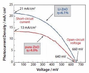
Figure 9.Photovoltaic behavior of ZnO films consisting of aggregates synthesized in the presence (denoted as “Li-ZnO”) and absence (denoted as “pure-ZnO”) of lithium salt.
Figure 9 shows the typical photovoltaic behavior of ZnO films consisting of aggregates synthesized in the presence and absence of lithium ions. These two types of films display similar open-circuit voltages (VOC) in the range of 640-660 mV and fill factors (FF) of 0.44- 0.48. However, they differ in short-circuit photocurrent densities (ISC), i.e., 13 mA/cm2 for pure-ZnO and 21 mA/cm2 for Li-ZnO. The larger photocurrent density leads to higher conversion efficiency. The efficiency of the Li-ZnO film reached 6.1%, while a value of 4.0% was attained for the pure-ZnO film. Such a significant enhancement in the conversion efficiency was ascribed to the use of lithium ions during the ZnO aggregate synthesis, which offered a positive influence on the solar cell performance by affecting the morphology, structure, and surface chemistry of the aggregates, and thus resulted in increased dye adsorption and more effective light scattering.
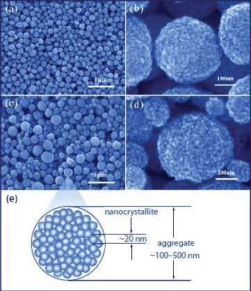
Figure 10.Morphology and structure of ZnO aggregate films. Images (a) and (b) are SEM images with different magnifications for the pure-ZnO film. Images (c) and (d) are SEM images of the Li-ZnO film, and (e) is a drawing to illustrate the hierarchical structure of the aggregates consisting of ZnO nanocrystallites.
Shown in Figure 10 are the SEM images of pure-ZnO and Li-ZnO films. An apparent difference in the morphology can be seen under low magnification (Figure 10a and Figure 10c). The pure-ZnO film is comprised of aggregates with a monodisperse size distribution, whereas the Li-ZnO film exhibits a broad distribution of aggregate size from several tens to several hundreds of nanometers. The different polydispersity of ZnO aggregates synthesized in the presence of lithium salt reflects the important influence of lithium ions on the growth of ZnO aggregates. It is possible that these lithium ions adsorb on the ZnO surface so as to mediate the agglomeration of ZnO nanocrystallites. A polydisperse size distribution of Li-ZnO aggregates is beneficial to light scattering, and it was thought to contribute to the light harvesting efficiency of the photoelectrode and partially resulted in an increase in the conversion efficiency of the cells. The difference of pure-ZnO and Li- ZnO films in the light scattering ability was confirmed by measuring optical absorption spectra of these two films. The results are shown in Figure 11. It can be seen that both films present an intrinsic absorption band at wavelengths below 385 nm and an additional absorption hump in the visible region. The latter is thought to be a result of light scattering, which causes light extinction via diffuse reflection and/or diffuse transmission. This affects the film transparency and appears in the spectra as pseudo-absorption. For the Li-ZnO film, it shows that the absorption in the visible region is stronger than that of the pure-ZnO. This is just because the aggregates in the Li-ZnO film are highly polydisperse in size and may generate more efficient light scattering than the monodisperse aggregates.
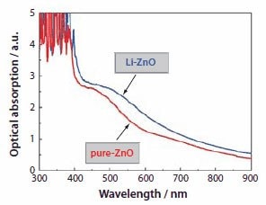
Figure 11.Optical absorption spectra of pure ZnO and Li-ZnO films.
Besides enhanced light scattering effect due to the polydispersity of ZnO aggregates in size, the use of lithium ions in the synthesis was also mentioned to increase the nanocrystallite size of ZnO and the pore size of aggregates. This offered a more porous structure for dye infiltration and electrolyte diffusion. Furthermore, the presence of lithium ions might also enhance the surface stability of ZnO, which which would prevent the formation of Zn2+/dye complexes and favor dye adsorption on ZnO in a monolayer. All these factors were thought to be helpful to improving the solar cell performance. It is worth noting that these samples were characterized through X-ray photoelectron spectroscopy (XPS). No detectable difference could be found in the XPS spectra for the pure-ZnO and Li-ZnO films, indicating that these two films are identical with regards to chemical composition. In other words, it excludes the possibility that lithium exists in the ZnO as a dopant or forms a composite with ZnO, although the term "Li-ZnO" is used to represent the ZnO aggregates that are synthesized in the presence of lithium ions.
Atomic Layer Deposition of TiO2 on ZnO Surface
Besides lithium ions that may mediate the growth and thus change the surface of the ZnO aggregates, another way to improve the surface stability of ZnO aggregates in a ruthenium complex dye is to deposit a thin film on the ZnO surface to form a core/shell structure.48 Atomic layer deposition (ALD) is an ideal technique for creating the core/shell structure due to its unique self-limiting nature and low growth temperature, which make it possible to apply an ultra-thin layer on porous structures.49,50 When ALD technique was employed to deposit an ultra-thin TiO2 layer on the porous ZnO aggregates, it significantly enhanced conversion efficiency of the solar cells. As illustrated schematically in Figures 12a-c, TiO2 ultra-thin layer deposited by ALD shows complete and conformal coverage on the surface and inside the pores of the aggregates. All of the dye molecules are adsorbed onto the surface of TiO2 coating. Such an ultra-thin and conformal ALD coating is so thin that it does not change the morphology of the underlying ZnO structures as shown in Figure 12e and Figure 12f. It was estimated that the thickness of the TiO2 coating layer after 10 cycles of ALD is 0.3–0.6 nm.51,52 The connections between adjacent ZnO nanocrystallites would remain to ensure a favorable electron motion through ZnO (as suggested in Figure 12d). Such a feature in the structure would improve the surface stability of the ZnO aggregates with enhanced dye loading, while retaining the advantage of high electron mobility of ZnO.
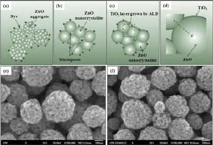
Figure 12.Schematics illustrating (a) ZnO aggregates adsorbed with dye molecules, (b) ZnO nanocrystallites containing micropores, (c) conformal ALD-TiO2 thin layer on the surface of ZnO nanocrystallites, (d) enlarged schematic showing the details of conformal ALD-TiO2 coating on ZnO surface and the uninterrupted connection between adjacent ZnO nanocrystallites for efficient electron motion, and SEM images of photoelectrode films of (e) submicrion-sized aggregates of ZnO nanocrystallites and (f) submicron-sized aggregates of ZnO nanocrystallites coated with thin TiO2 layer.
A Brunauer-Emmett-Teller (BET)53 characterization of the TiO2-coated ZnO aggregates implies that micropores inside each aggregate still remain after the ALD treatment, indicating that the porous structure of the photoelectrode film is preserved. This is very important for the photoelectrode to achieve sufficient dye adsorption. Due to the introduction of TiO2 coating layer, a slight decrease in both the size and the volume of the micropores was observed. It was thought that the structure of ZnO aggregates with a TiO2 coating layer was able to suppress the recombination because of the formation of a n-n* heterojunction at the ZnO/TiO2 interface.54 This could be verified by the electrochemical impedance spectroscopy (EIS), which showed the suppressed recombination at the aggregate/electrolyte interface due to the coating of TiO2 layer. As a result, both the open circuit voltage and the fill factor of the cell were increased and, impressively, the conversion efficiency was improved from 5.2% to 6.3% (Table 2).55
Conclusions
ZnO aggregates were synthesized and studied as a photoelectrode material in DSCs. Such aggregates are formed by nano-sized crystallites, and thus possess extremely large surface areas. Simultaneously, the size of the aggregates is in the submicron range; which is comparable to the wavelength of the visible light and, therefore, the aggregates are very effective in light scattering. The existence of light scattering in a photoelectrode film may significantly extend the traveling distance of the light and as such enhance the light harvesting efficiency of the photoelectrode. This finally leads to an improvement in the conversion efficiency of a DSC with photoeletrode consisting of the aggregates. Typically, in the case of ZnO, the aggregates have presented an increase in the conversion efficiency of more than 120% compared with nanocrystallites, which are far smaller than the light wavelength in size and unable to generate light scattering.
A polydisperse distribution in the aggregate size might facilitate the generation of more intensive light scattering. The use of lithium ions to mediate the growth of the ZnO aggregates resulted in a polydisperse distribution and an improved surface stability of the ZnO in the ruthenium complex dye. The treatment of the ZnO aggregate film with an ALD technique for coating a TiO2 layer proved to be helpful in reducing the electron recombination due to the formation of a n-n* heterojunction at the ZnO/TiO2 interface. Both these surface modification methods have been verified to result in an increase in the conversion efficiency of the dye-sensitized ZnO aggregate solar cells from 5.2-5.4% to 6.2-6.3%. The use of nanocrystallite aggregates in the photoelectrode film for light scattering is anticipated to further improve the performance of DSCs based on TiO2, which have already achieved 10-11% conversion efficiencies.
Acknowledgements
This work is supported by the U.S. Department of Energy, Office of Basic Energy Sciences, Division of Materials and Engineering under Award No. DE-FG02-07ER46467 (Q.F.Z.), the Air Force Office of Scientific Research (AFOSR-MURI, FA9550-06-1-0326) (K.S.P.), the University of Washington TGIF grant, the Washington Research Foundation, and the Intel Corporation.
Materials
References
如要继续阅读,请登录或创建帐户。
暂无帐户?